Power Losses In Switches
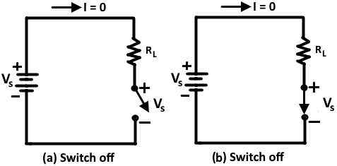
An ideal switch is shown in Figure 1. The power loss generated in the switch is the product of the current through the switch and the voltage across the switch. When the switch is off, there is no current through it (although there is a voltage VS across it). And therefore, there is no power dissipation. When the switch is on, it has a current (VS / RL) through it, but there is no voltage drop across it, so again there is no power loss. We also assume that for an ideal switch the rise and fall time of the current is zero. That is, the ideal switch changes from the off state to the on state (and vice versa) instantaneously. The power loss during switching is therefore zero.

Unlike an ideal switch, an actual switch, such as a bipolar junction transistor, has two major sources of power loss: conduction loss and switching loss.
Conduction Loss
When the transistor in Figure 2(a), is off, it carries a leakage current (lLEAK). The power loss associated with leakage current is POFF = VS x ILEAK . However, since the leakage current is quite small and does not vary significantly with voltage, it is usually neglected and thus the transistor power loss is essentially zero. When the transistor is on, as in Figure 2(b), it has a small voltage drop across it. This voltage is called the saturation voltage (VCE(SAT)). The transistor’s power dissipation or conduction loss due to the saturation voltage is:
PON = VCE(SAT) x IC
Where
IC = (VS - VCE(SAT)) / RL ≈ VS / RL
Equation 1 gives the power loss due to conduction if the switch remains on indefinitely. However, to control the power for a given application, the switch is turned on and off in a periodic manner. Therefore, to find the voltage power loss we must consider the duty cycle:
PON(avg) = VCE(SAT) x Ic x (ION / T) = VCE(SAT) x IC x d
Similarly
POFF(avg) = VS x ILEAK x tOFF / T
Here, the duty cycle d is defined as the percentage of the cycle in which the switch is on:
d = tON / (tON x tOFF ) = tON / T

Switching Loss
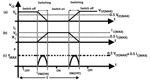
In addition to the conduction loss, a real switch has switching losses because it cannot change from the on state to the off state (or vice versa) instantaneously. A real switch takes a finite time tSW(ON)to turn on and a finite time tSW(OFF)to turn off. These times not only introduce power dissipation but also limit the highest switching frequency possible. The transition times tSW(ON) and tSW(OFF)for real switches are usually not equal, with tSW(ON) generally being larger. However, in this discussion we will assume that tSW(ON) is equal to tSW(OFF). Figure 3. Shows switching waveforms for (a) the voltage across the switch and (b) the current through it. When the switch is off, the voltage across it is equal to the source voltage. During turn-on, which takes a finite time, the voltage across the switch decreases to zero. During the same time, the current through the switch increases from zero to IC. The transistor has a current through it and a voltage across it during the switching time; therefore, it has a power loss.

To find the power dissipated in a transistor during the switching interval, we multiply the instantaneous value of IC and the corresponding value of VCE. the instantaneous power curve is shown in Figure 3(c). the energy dissipated in the switch is equal to the area under the power waveform. Note that the maximum power is dissipated when both the current and the voltage are passing through their midpoint values. Therefore, the maximum power loss when switching from the off state to the on state is:
PSW ON(max) = 0.5 VCE(max) x 0.5 IC(max)
It is interesting to note that the power curve looks essentially like a rectified sine wave. The average value of this waveform is
PSW ON(avg) = 0.637 x PSW ON(max)
= 0.637 x 0.5 VCE(MAX) x 0.5 IC(MAX)
= 0.167 VCE(max) x IC(max)
Or
PSW ON(avg) = 1/6 VCE(max) x IC(max)
The energy loss (power x time) during turn on will be PSW ON(avg) x tSW(ON)
WSW ON = 1/6 VCE(max) x IC(max) x tSW(ON) (joules)
A similar analysis gives the energy loss during turnoff as
WSW OFF = 1/6 VCE(max) x IC(max) x tSW(ON) (joules)
The total energy loss in one cycle due to switching is given by
WSW = WSW ON + WSW OFF + 1/6 VCE(max) x IC(max) x [tSW ON + tSW OFF]
The average power dissipation in the switch will be
PSW = WSW/T = WSW x f
PSW = 1/6 VCE(max) x IC(max) x [tSW ON + tSW OFF] x f
Where T is the switching period and f is the pulse repetition rate (frequency of switching). Note that
T = tON + tSW(ON) + tOFF + tSW(OFF)
If we let
tSW(ON) = tSW(ON) tSW(OFF) = tSW
then
PSW = 1/6 VCE(max) x IC(max) x (2 tSW) x f
The total power loss in switch is
PT = PON(avg) + POFF(avg) + PSW
≈ PON(avg) + PSW
= d x VCE(sat) x IC 1/3 x VCE(max) x IC(max) x tSW x f
Related Articles
Voltage Current Characteristic of Diode
