BJT Bipolar Junction Transistor
This name is a representation for a device having transfer resistors. As we have seen a semiconductor offers less resistance to flow of current in one direction and high resistance in another direction, we call the device made of semiconductors as a transistor.
There are basically two types of transistors:
- Point contact
- Junction transistor
Junction transistors are more in use compared to point type transistors. They are preferred due to their ruggedness and small size. Junction transistors are further classified into two types
- PNP
- NPN
Each has 3 electrodes called emitter, base, and collector. These are made of P and N types semiconductors depending on the type.
TRANSISTOR
The transistor was invented by William Shockley in 1947. A transistor consist of two PN junctions. The junctions are formed by sandwiching either P-type or N-type semiconductor layers between a pair of opposite types. There are two types of transistors one is called PNP transistor and other is called NPN transistor.
A PNP transistor is composed of two P-type semiconductors separated by a thin section of N-type as shown in Figure (a). Similarly, NPN transistor is composed of two N-type semiconductors separated by a thin section of P-type as shown in Figure (a). the symbol used for PNP and NPN transistors are also shown with the diagrams.
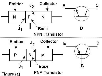
Basically, transistor has three portions known as emitter, base and collector. The portion on one side is the emitter and the portion on the opposite side is the collector. The middle portion is called the base and forms two junctions between the emitter and collector.
EMITTER
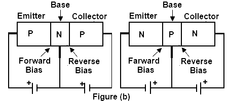
The portion on one side of transistor that supplies charge carriers (i.e. electrons or holes) to the other two portions. The emitter is a heavily doped region. The emitter is always forward biased with respect to base so that it can supply a large number of majority carriers. In both PNP and NPN transistors emitter base junction always should be forward biased. Emitter of PNP transistor supplies hole charges to its junctions with the base. Similarly, the emitter of PNP transistor supplies free electrons to its junction with the base.
COLLECTOR
The portion on the other side of the transistor (i.e. the side opposite to the emitter) that collects the charge carriers (i.e. electrons or holes). The collector is always larger than the emitter and base of a transistor. The doping level of the collector is in between the heavily doping of emitter and the light doping of the base. In both PNP and NPN transistors the collector base junction always should be reverse biased. It function is to remove charge carriers from junction with the base. Collector of PNP transistor receives hole charges that flow in the output circuit. Similarly, the collector of NPN transistor receives electrons.
BASE
The middle potion which forms two PN junctions between the emitter and the collector is called the base. The base of transistor is thin, as compared to the emitter and is a lightly doped portion. The function of base is to control the flow of charge carrier. The emitter junctions forward biased, allowing low resistance emitter circuit. The base collector junction is reverse biased and showing high resistance in the collector circuit.
TRANSISTOR CONSTRUCTION
The techniques used for manufacturing transistor are given as below:
- Grown Junction
- Alloy or Fused Junction
- Diffused Junction
- Epitaxial Junction
- Point Contact Junction
Grown Junction
This junction is prepared by using either the Czochralski or floating zone technique. The apparatus used for Czochralski technique is shown in the below Figure. It consists of a graphite crucible, a quartz container, a rotating pulling rod and the induction heating coils placed around the graphite crucible. The graphite crucible contains the molten semiconductor material.

Apparatus for Czochralski Technique
First of all, a single semiconductor seed is immersed in the molten semiconductor. Then it is gradually withdrawn, while the rod holding the seed is slowly rotating. The PN junctions are grown by first adding P-type impurities to the melt and then changing it to N-type.
Alloy or Fused Junction
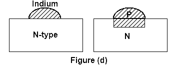
The alloy junction technique produces PN junctions, which have high (PIV) peak-in-voltage and current ratings. Such junctions have large capacitance, due to their large junction area. In the alloy junction technique, a small dot of aluminum is placed on the N-type silicon water as shown in Figure (d). It is ten heated to temperature of about 150C. At this temperature, the aluminum melts and dissolves some of the silicon. Then its temperature is lowered and silicon refreezes to form a single crystal having a PN junction as shown in Figure.
Diffused Junction
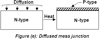
This technique gives us a precise control of impurity concentration for manufacturing PN junction. N-type silicon wafer called substrate (or base) is exposed to a gaseous impurity of P-type as shown in Figure (e). Then the wafer is heated to a sufficiently high temperature at which the impurities diffuse slowly into the surface of the water. After the diffusion, portions of the surface are protected and the rest are etched out as shown in Figure.
Epitaxial Junction
This junction differs from diffused junction only in one aspect that the junction is fabricated not on the substrate but on the epitaxial layer grown, above the substrate. The epitaxial junctions have an advantage of low resistance.
Point Contact Junction
It consists of an N-type semiconductor (silicon, or germanium) wafer, whose one face is soldered to a metallic base and the other face has a phosphor bronze (or tungsten) spring (called Cat’s whisker) pressed against it as shown in Figure (f). The whole assembly is encapsulated in a ceramic or glass envelops to give it mechanical strength.
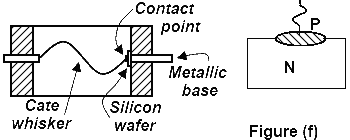
The PN junction is formed by passing a large current (about 200 mA) for 1 to 100 millisecond duration. The junction is formed at the contact point because of the melting of silicon surface and diffusion of the whisker material into the surface at that point as shown in Figure (f).
The point contact junction has very low value of the capacitance. Because of this, such junctions are very useful for operation at the frequencies as high as 10 GHz.
BJT Modes of Operation
There are two junctions in bipolar junction transistor. Each junction can be forward or reverse biased independently. Thus there are four modes of operations:
- Forward Active
- Cut off
- Saturation
- Reverse active
FORWARD ACTIVE
In this mode of operation, emitter-base junction is forward biased and collector base junction is reverse biased. Transistor behaves as a source. With controlled source characteristics the BJT can be used as an amplifier and in analog circuits.
CUTT OFF
When both junctions are reverse biased it is called cut off mode. In this situation there is nearly zero current and transistor behaves as an open switch.
SATURATION
In saturation mode both junctions are forward biased large collector current flows with a small voltage across collector base junction. Transistor behaves as an closed switch.
REVERSE ACTIVE
It is opposite to forward active mode because in this emitter base junction is reverse biased and collector base junction is forward biased. It is called inverted mode. It is no suitable for amplification.
However the reverse active mode has application in digital circuits and certain analog switching circuits.
