Formation of Depletion Layer in Diode
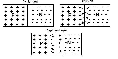
There is greater concentration of holes in P-region and electrons in N-region. This difference in concentration establishes a density mismatch across the junction resulting in majority carrier diffusion Holes diffuse from P to N and electrons from N to P regions causing the recombination.

This recombination of electrons and holes produces a narrow region at junction called depletion layer.
Potential Barrier
As the depletion layer built up a different of potential appears across the junction this difference of potential at junction is called potential barrier. The value of potential barrier VB is 0.3 volt for germanium and 0.7 Volts for Silicon.
Forward Bias

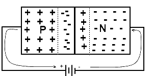
When a P-region of a semiconductor diode is connected with the positive terminal of battery and the N-region with negative terminal of the battery then the PN Junction is said to be forward biased.
Reverse Bias
When a P-region of a semiconductor diode is connected with the negative terminal and N-region with the positive terminal of the battery then the PN Junction is said to be reverse biased

In reverse bias the holes are attracted toward the negative terminal of the battery and the electrons are attracted towards the positive terminal of the battery causing the majority carrier both holes and electrons move away form the junction and each other.
Characteristics of PN Junction

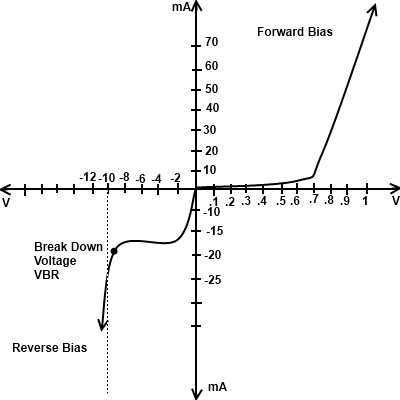
When the diode is forward biased and the applied voltage is increased from zero hardly any current flows through the diode in beginning, because the external voltage is being oppose by the internal barrier voltage (VB) whose value is 0.7 Volt for silicon and 0.3 Volt for Germanium. It is seen that when the voltage approaches to one volt (1V) a high forward current flows through the diode.
When the diode is in reverse bias majority carrier are block and only a small current due to minority current flows through the diode. As the reverse voltage is increase from zero the reverse current very quickly reaches its maximum or saturation value Io which is known as leakage. When reverse voltage exceeds a certain value which break down the the diode and huge amount of current flow through diode. This voltage is called break down voltage.
Maximum Forward Current
The highest current which a junction can conduct with out damaging it is called maximum forward current
Peak Inverse Voltage (PIV)
Peak inverse voltage PIV is the maximum reverse voltage that can be applied to the PN Junction with out damaging the junction.
Maximum Power Rating
It is maximum power rating is the maximum power that junction dissipate with out being over heated
Applications of PN Junction Diode
- It is mostly used as rectifier
- In Communication for modulation and demodulation
- In Logic Circuits
