Hybrid Equivalent of Transistor
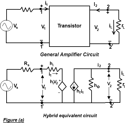
Figure(a) shows a transistor amplifier circuit. Such circuit can be connected in any one of the three configuration called common emitter, common base or common collector to a voltage source (Vs) and load resistance (ri). The voltages source has an internal resistance (Rs) as shown in figure. The load resistance (rL)) is the effective or A.C load resistance seen by the transistor at its output. Figure (a) shows the hybrid formulas for input resistance, output resistance, current gain and voltage gain of a transistor.

The expression for transistor amplifier input and output resistances, voltage and current gains may be obtained from the relations:
Vi = h1.i1 + hr.V2 ---------------(1)
i2 = hf.i1 + ho.V2 ----------------(2)
The voltage drop across load resistance (rL) is equal to the voltage across the output terminals of atransistor.
V2 = iL.rL = -i2.rL (Since i2 = -iL)
Current Gain
It is the ratio of output current (iL) to input currents (i1). Mathematically, the current gain,
Ai = i1/i1 = i2/i1
Putting the value of V2 (equal to –i2.rL) in equation (2)
i2 = hf.i1 + ho(-i2.rL) = hf.i1 –ho.i2.rL
i2 + ho.i2.rL = hf.i1
i2(1 + ho.rL) = hf.i1
i2/i1 = hf/(1 + ho.rL)
Ai = i2/i1 = -(hf/(1 + ho.rL)) -------------------(3)
Input Resistance
Input resistance value is given by the ratio of input voltage (V1) to the input current (i1).
Mathematically,
Ri = V1/i1
Again putting the value of V2 (equal to –i2.rL) in equation (1)
V1 = hi.i1 + hr(-i2.rL)
= hi.i1 – hr.i2.rL
Dividing the equation (1) by i1 on both sides,
V1/i1 = (hi.i1 – hr.i2.rL)/i1 =hi – hr(i2/i1)rL
Replacing v1/i1 with Ri and i2/i1 by –Ai in the above equation.
Ri = hi – hr(-Ai).rL = hi + hr.Ai.rL --------------(4)
Putting the value of Ai equal to –hf/(1 + ho.rL) from equation (3) in the above expression.
Ri = hi + hr (-(hf/(1 + ho.rL)rL)
= hi – (hr.hf/ho + (1 / rL)) ----------------- (5)
Voltage Gain
It is defined as the ratio of output voltage (V2) to the input voltage (V1).
Mathematically, the voltage gain,
Av = V2/V1 = -(i2.rL/V1) (as V2 = -i2.rL)
Putting the value of i2 (equal to –Ai.i1) from equation (2) the above expression,
Av = (Ai.i1.rL/V1) = Ai.rL(i1/V1)
Replacing i1/V1 by Ri in the above expression,
A = Ai.rL/Ri
Putting the value of Ai (equal to –hf/(1 + ho.rL) and Ri (equal to hi – hr/hf(ho + 1/rL)) in the above expression and re-arranging,
Av = - ( hf.rL/(hi + (hi.ho – hr.hf)r1))
If we replace (hi.ho – hr.hf = ∆h) in the above expression then the voltage gain,
Av = -( hr.rL/ (hi + ∆h.rL))
Output Resistance
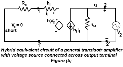
It is obtained by setting the source voltage (Vs) to zero and the load resistance (rL) to infinity and by driving the output terminals from a source V2 as shown in below Figure (b).

Then output resistance is the ratio of voltage (V2) to the current drawn from the voltage source (i2).
Mathematically, the output resistance,
Ro = V2/i2 = (V2/(hr.i1 + ho.V2) ------------(6)
The value of current (i1) can be obtained by applying Kirchhoff’s Law to the input side of transistor amplifier circuit.
Rs.i1 + hi.i1 + hr.V2 = 0
As i1 = -(hr.V2)/ (Rs + hi)
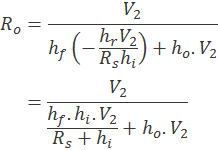
Putting this value of i1 in equation (6)

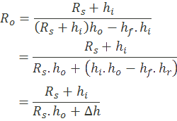
Rearranging the above equation

If source resistance (Rs) is zero, then output resistance is,
Ro = hi/∆h
Power Gain
It is defined as the product of voltage gain (Av) and the current gain (∆i).
Mathematically, the power gain is,
∆p = Av.Ai
