Integrated Components In IC
INTEGRATED TRANSISTORS
How transistor, capacitor, resistor and diodes are fabricated on a chip. The steps involved in fabrication of a semiconductor devices on a chip are discussed below in detail.
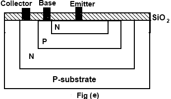
Fig.(a) shows how these steps are applied to fabricate NPN transistor.
Epitaxial growth.
Create SiO2 layer (oxidation)
Open window in SiO2 and perform boron diffuse to create P-layer.
Oxidation again, open window in new SiO2 layer perform phosphorus diffusion to create N-layer.
Oxidize again, open windows for base, emitter and collector contact. Metallization deposit Al, remove all except in contact regions.
Step-1
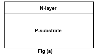
First of all an N-type silicon layer of about 5 to 25 µm (1 µm = 10-6 m) thick is grown on the P-type substrate. The N-type layer is grown by placing the wafer in a special furnace called reactor at 900 to 1200°C. This process is called Epitaxial as shown in Fig. (a).
Step-2
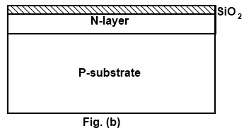
A thin layer of silicon dioxide SiO2 is grown over the N-type layer by exposing the wafer of an oxygen atmosphere at about 1000°C. The thickness of silicon dioxide SiO2 layer is generally in the range of 0.02 to 2 µm. This layer is commonly called an insulating layer or oxide layer. This process is called oxidation as shown in Fig. (b).
Step-3
After oxidation again, the wafer is coated with a uniform film of a photosensitive emulsion or etching solution. This process is called photolithography. A layout of the desired ice pattern to opens the windows is made. This negative or stencil of the required dimensions is placed as a mask over the photoresist. By exposure of the emulsion to ultraviolet light through the mask, the photoresist becomes polymerized under the transparent regions of the stencil. The mask is now removed and the wafer is developed by using a chemical called trichloroethylene. This chemical dissolves the unexposed portions of the photoresist film and leaves the surface pattern.
The wafer is now immersed in an etching solution by hydrofluoric acid. This acid removes the oxide from the areas through which the impurities are to be diffused.
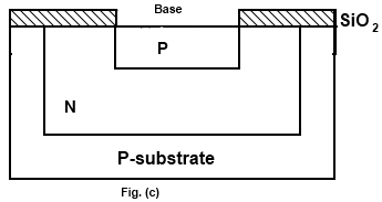
The next step is to introduce impurities such boron in the wafer by diffusion process to create P-layer. In this process, the wafer is placed in a high temperature furnace (of about 100°C) and P-type impurities are diffused into N-type layer as shown in Fig. (c). The P-type base of the transistor is now diffused in to the N-layer, which acts as a collector.
Step-4
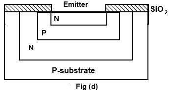
After that the oxidation, the photoresist and masking process is repeated. This creates windows in the silicon dioxide layer as shown in Fig. (d). The next is to introduce impurities such as phosphorus by similar diffusion process i.e., N-type emitter is now diffused into the base of P-type layer as shown in Fig. (d).
Step-5
After that the oxidation and open windows for base, emitter and collector contact. Metallization is necessary, for making interconnections and providing bonding pads around circumference of the chip for connection of wires. The metallization is done by vacuum evaporation of aluminum and then selectivity etching away the aluminum over the entire surface.
INTEGRATED DIODE
Fig. (f) Shows the cross section area of the integrated diode.
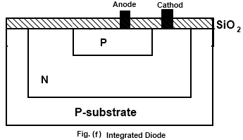
Integrated diode is constructed by bipolar transistor fabrication process. N-type epitaxial layer is grown on the P-type substrate. A thin layer of silicon dioxide SiO2 is grown over the N-type layer i.e. a N-type which is greater in size is diffused into the P-type substrates which acts as a cathode and a their oxide layer is grown. P-type impurities which are small in size are diffused into N-type layer. Again the entire wafer is now covered with silicon dioxide. Using masking and etching techniques, the, contact surfaces for the device terminals are defined. The entire wafer is now covered by aluminum layer and final mask defines the desired interconnection pattern. The excess aluminum is removed by etching technique. This completes the fabrication process of diode.
TRANSISTOR CONNECTED AS DIODE
There are number of ways in which a transistor can be connected as a diode as shown in Fig. (g). They are obtained from a transistor structure by using; the emitter-base diode, with the collector shorted to the base the emitter-base diode with the collector open; the collector-base diode with the emitter open as shown in Fig. (g) respectively.
INTEGRATED CAPACITORS
The capacitors in monolithic integrated circuits are fabricated in two basic methods one is the depletion-region (or junction0 by utilizing capacitance of a reverse biased PN junction, the MOS transistor or their film deposition.
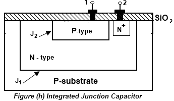
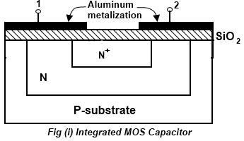
As in the case of diodes and resistors, it is desirable to make junction capacitors during one of the transistor diffusion steps. The base-collector junction of a transistor, without emitter diffusion can be used as a capacitor. The emitter-base junction can also be used, or on N+ region can be diffused into one of the P isolation region during an emitter diffusion. Fig. (h) shows the structure of a junction capacitor utilizing the base-collector junction of a transistor Fig. (i) shows a MOS non-polarized parallel plate (b) capacitor. This capacitor utilizes silicon dioxide layer as a dielectric. A Thin film of aluminum acts as a top plate. The bottom plate consists of heavily doped N+ region, which is formed during either the emitter diffusion in bipolar, process or the implantation of the drain and source regions in MOS process.
The junction capacitor type has a drawback that the value of capacitance varies with the voltage. The capacitance of MOS or junction capacitor is up to about 100 pF. The use of tantalum films can increase its capacitance.
INTEGRATED RESISTOR
The resistors in monolithic ICs are usually obtained by utilizing the bulk resistivity of one of transistor region. Most of to the resistor are made during the diffusion of base as shown in Fig. (j) because base is high resistivity. The resistor can also be made using resistivity of any diffusion areas. Most resistor uses P-type base diffusion region. However emitter’s diffusion can also be used. Since resistivity of emitter region is very low and hence to make low resistance values emitter region are used.
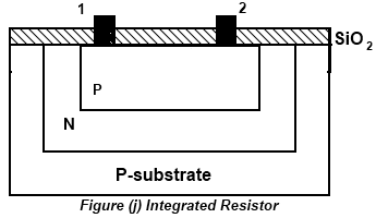
In order to make integrated resistor first of all N-type epitaxial layer is grown on the P-type substrate and then a P-type impurities which in to N-type layer. Fig. (j) Shows the structure of diffused resistor. The resistance of P-region depends upon its length, width, depth of diffusion and resistivity of the diffused material. The resistance of diffused layer is given by
R = Ω (L/A) = Ω (L/W.t)
Where
Ω = Average resistivity of diffused layer
L = Length of diffused layer
W = Width of diffused layer
t = Thickness of diffused layer and
A = Cross-sectional area of diffused layer
The range values obtainable with diffused resistors are limited by the size of the area required by the resistor. Practical range of resistance is 20 Ω to 30 k Ω for an emitter diffused resistor.
