Schmitt Trigger
Schmitt trigger belongs to a class of bistable multivibrator circuits. In a bistable, there exist two D.C. couplings from each output to input of the other. But in Schmitt trigger circuit, there exists only one coupling. It can be recalled that if in the emitter coupled bistable the feedback network from the collector of transistor Q2 to the base of transistor Q1 is removed , it becomes a Schmitt trigger circuit.
The Schmitt trigger is used for wave shaping circuits. It can be used for generation of a square wave from a sine wave input. Basically, the circuit has two opposite operating states like in all other multivibrator circuits. However, the trigger signal is not, typically, a pulse waveform but a slowly varying A.C. Voltage. The Schmitt trigger is level sensitive and switches the output state at two distinct trigger levels. One of the triggering levels is called a lower trigger level (abbreviated as L.T.L) and the other as upper trigger level (abbreviated as U.T.L).

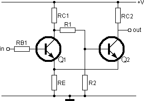
Figure 1 shows the circuit of a Schmitt trigger, the circuit of Schmitt trigger contains of two identical transistors Q1 and Q2 coupled through an emitter RE. The resistor R1 and R2 form a voltage divider across the VCC supply and ground. These resistors provide a small forward bias on the base of transistor Q2.
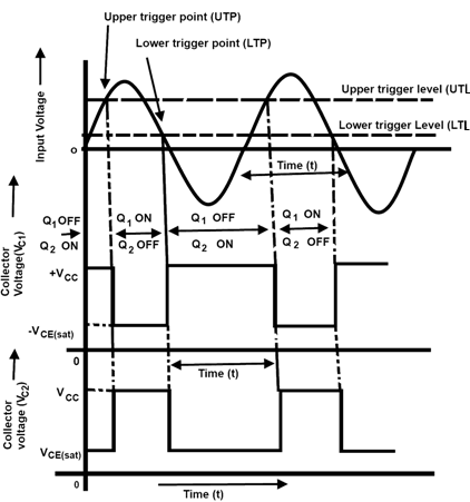
Let us suppose that initially there is no signal at the input. Then as soon as the power supply VCC is switched on, the transistor Q2 starts conducting. The flow of its current through resistor RE produces a voltage drop across it. This voltage drop acts as a reverse bias across the emitter junction of transistor Q1 due to which it cuts-off. As a result of this, the voltage at its collector rises to VCC. This rising voltage is coupled to the base of transistor Q2 through the resistor R1. It increases the forward bias at the base of transistor Q2 and therefore drives it into saturation and holds it there. At this instant, the collector voltage, level are VC1 = VCC and VC2 = VCE(sat) as shown in Figure 2.

Now suppose an A.C. signal is applied at the input of the Schmitt trigger (i.e. at the base of the transistor Q1). As the input voltage increases above zero, nothing will happen till it crosses the upper trigger level (U.L.T). As the input voltage increases, above the upper trigger level, the transistor Q1 conducts. The point, at which it starts conducting, is known as upper trigger point (U.T.P). As the transistor Q1 conducts, its collector voltage falls below VCC. This fall is coupled through resistor R1 to the base of transistor Q2 which reduces its forward bias. This in turn reduces the current of transistor Q2 and hence the voltage drop across the resistor RE. As a result of this, the reverse bias of transistor Q1 is reduced and it conducts more. As the transistor Q1 conducts more heavily, its collector further reduces due to which the transistor Q1 conducts near cut-off. This process continues till the transistor Q1 is driven into saturation and Q2 into cut-off. At this instant, the collector voltage levels are VC1 = VCE(sat) and VC2 = VCC as shown in the figure.
The transistor Q1 will continue to conduct till the input voltage falls below the lower trigger level (L.T.L). It will be interesting to know that when the input voltage becomes equal to the lower trigger level, the emitter base junction of transistor Q1 becomes reverse biased. As a result of this, its collector voltage starts rising toward VCC. This rising voltage increases the forward bias across transistor Q2 due to which it conducts. The point, at which transistor Q2 starts conducting, is called lower trigger point (L.T.P). Soon the transistor Q2 is driven into saturation and Q1 to cur-off. This completes one cycle. The collector voltage levels at this instant are VC1 = VCC and VC2 = VCE(sat). No change in state will occur during the negative half cycle of the input voltage.
It is proved from the above discussion that the output of a Schmitt trigger is a positive going pulse, whose width depends upon the time during which transistor Q1 is conducting. The conduction time is set by the upper and lower trigger levels.
Op-Amp Schmitt Trigger
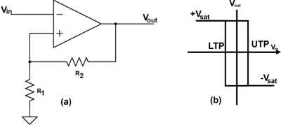
Figure 3 (a) shows an op-amp Schmitt trigger. Because of the positive feedback to the non-inverting input, the output is saturated in either the positive or negative direction. Assume the output is positively saturated. Then a positive voltage is fed back to the non-inverting input. This positive voltage is called upper trip point (UTP). As long as the inverting input voltage is less than UTP, the output voltage remains positively saturated. This means the operating point is somewhere along the upper part of the graph in Figure 3 (b).
If we slowly increase the input voltage, we eventually reach a point where it is slightly more positive than the UTP. When this happens, the error voltage changes polarity, driving the op-amp into negative saturation. With the output now negative, the voltage divided feeds back a negative voltage to the non-inverting input. This negative voltage is referred to as the lower trip point (LTP).
The output remains in negative saturation as long as the input voltage is more negative than the LTP. The only way to change the output is to decrease the input voltage untill it is slightly more negative than LTP. Then the error voltage changes polarity and the output switches back to positive saturation.
The formulas for the trip points are

Generating Square Waves
One way to generate square wave is to drive a Schmitt trigger with a sive wave whose positive peak is greater than the UTP and whose negative peak is less than the LTP.
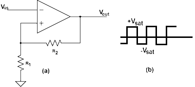
For instance, Figure 4(a) shows a Schmitt trigger with equal resistor in the voltage divided. This means the UTP is
Similarly, the LTP equals -Vsat / 2. If Vsat is 10V, then UTP is +5V and LTP is -5V. If the sine wave shown in Figure 4(b) has a positive peak greater than +5V and a negative peak less than -5V, then the Schmitt trigger produces the square wave output shown in Figure 4(b).
The shape of the input signal is immaterial. Instead of a sine wave, any periodic signal with sufficient amplitude to drive the Schmitt trigger will result in an output square wave like Figure 4(b).

