Phototransistor
The phototransistor has a light sensitive collector base PN junction. It is exposed to incident light through a lens opening in the transistor package. When there is no incident light, there is a small thermally generated collector to emitter leakage current, this is called dark current. When light strikes the collector base PN junction a base current (Iλ) is produced that is directly proportional to the light intensity. This action produces a collector current that increases with base current (Iλ). The relationship between the collector current and the base current schematic symbol is known in figure.

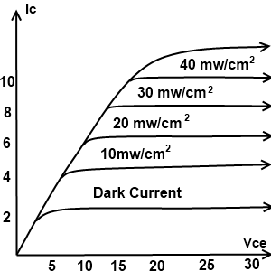
Since, the actual photo generation of base current occurs in the collector, base region, the larger the physical area of this region, the more base current is generated. A photo transistor with a biasing circuit and typical collector characteristic curve is shown in figure.


Notice that each individual curve in the graph corresponds to a certain value of light intensity and that the collector current increases with light intensity.
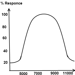
Phototransistors are not sensitive to all light but only to light within a certain range of wavelengths. They are most sensitive to particular wavelengths.

