FET or JFET
FET stands for "Field Effect Transistor" it is a three terminal uni polar solid state device in which current is control by an electric field.

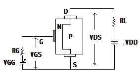
FET can be fabricated with either N- Channel or P- Channel, for the fabrication of N-Channel JFET first a narrow bar of N-type of semiconductor material is taken and then two P-Type junction are defused on opposite sides of it's middle part, called channel. The two regions are internally connected to each other with a signal lead, which is called Gate terminal. One lead is called Source terminal and the other is called Drain terminal.Construction of FET
P-Channel JFET is similarly is constructed except that it use P- type of bar and two N- types of junctions.
Source:-
It is the terminal through which majority carriers are entered in the bar, so it is called Source.
Drain:-
It is the terminal through which the majority carriers leads the bar, so it is called the drain terminal.
Gate:-
These are two terminals which are internally connected with each other and heavily doped regions which form two PN-Junctions.
Working / Operation FET or JFET
Gate are always in reverse biased, hence the gate current IG is practically zero. The source terminal is always connected to end of the drain supply, which provides the necessary carrier, in N- Channel JFET Source terminal is connected to the negative end of the drain voltage source. The electrons flow from source to drain through the channel from D to S is started,

the current ID increases as VDS is increased from zero on ward. This relation ship between VDS and ID continuous till VDS reaches certain value called "Pinch OFF" VPO.
When VDS is equal to zero and VGS is decreased from zero, the gate reverse bias increases the thinks of the region, as the negative value of the VGS is increase a stage cones when the two dip lections regions touch each other, in this conduction the channel is said to be Cut OFF.
JFET as Amplifier
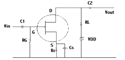
One of the application of the JFET is an Amplifier, it amplified the weak signal connected in the Gate terminal , the input is always reversed biased, a small change in the reverse bias on the gate produce large change in the drain current, this fact make JFET capable of amplifing the weak signals
Working / Operation
When negative signal is applied at in put of the amplifier, the gate bias is increase, duplication layer is decrease, Channel resistance is increase, ID is decreased, Drop across Load Resistor is decreases, and the positive signal is present at output through C2.
When the positive signal is applied at the input the action will be the wise versa
This seen that there is phase inveration between the input signal at the gate and the output signal at the drain.
Application of JFET
JFET is used at large scale in amplifiers circuits, analog switches; it is also used in AGC system, voltage regulators, buffer amplifiers.
MOSFET
The MOSFET is sub divided in to two types,
- DE-MOSFET
- E only MOSFET
DE- MOSFET
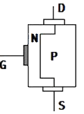
This MOSFET could be operating in both duplication and Enhancement mode. By Changing the Polarity o VGS, when VGS is negative for the N-Channel DE- MOSFET is operate in depletion mode, however with positive gate voltage it operates in an Enhancement mode.
E- Only MOSFET
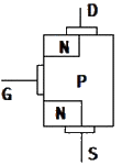
This MOSFET Operates in the only Enhancement mode. It differs only in construction from the DE- MOSFET in that there exists no channel between the drain and source.
DE-MOSFET Construction
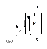
Like JFET it has source, Gate and Drain, However its gate is insulated from its conduction channel by an ultra thin metal oxide. Insulating film usually silicon dioxides (SiO2), because of this insulating property MOSFET is also known as Insulated Gate Field Effect Transistor (IGFET). In DE-MOSFET we can apply both the positive and negative voltages at gate terminal because the gate terminal is isolated from the channel.
DE-MOSFET Working / Operation
Depletion Mode

When VGS=0 electrons can flow freely from source to drain through the conduction channel, When a negative voltage is applied at gate terminal, it depletes the N- channel and its electrons by inducing positive charges in it. Grater negative voltage on the gate, grater is the reduction in the number of electrons in the channel which increase the conduction. In fact too much negative gate voltage cut off the channel, thus with negative gate voltage a DE-MOSFET behaves like a JFET, for this reason negative gate operation of DE-MOSFET is called Depletion mode Operation.
Enhancement Mode
In circuit diagram the drain current flows from source to drain even with zero gate bias, when positive voltage is applied to the gate, the input gate capacitor is able to create pre- electrons in the channel which increase the ID. Pre- electrons are induced in the channel by the capacitor action, these electrons are added to the other ready electrons for the conduction, which increase the number of electrons and these electrons increase the conductivity of the channel.
As positive gate voltage increases the number of induced electrons is increased which increase the conductivity of channel from source to drain, this way the current is also increased. The positive gate operation of the DE-MOSFET is known as enhancement mode.
Application of MOSFET
MOSFET have wide application in field of electronics some of these application are given below.
- As input amplifier in oscilloscope, electronic volt meter, and other measuring and testing equipment because they have high input resistance.
- It is used In logic circuits for fast switching.
- It is also used in TV receiver.
- It is used in computer circuits.
- In high frequency amplifiers.
