Inverting & Non-Inverting Amplifiers
INVERTING AMPLIFIER
A inverting amplifier provides the same function as the common emitter and common-source amplifiers. The schematic diagram for an inverting amplifier is shown in Figure (a).
Observe that the offset and D.C. voltages have been left off of these circuits for simplicity. These connections are generally the same for all circuits using the same type of OP-AMP.
The input signal is applied to the inverting (minus) input. The (-) input produces a 180o phase shift between input and output signal. The non-inverting (plus) input is grounded and is common to both the input and the output.
Negative feedback (degenerative) is coupled from the output back to the input through the feedback resistor (Rf). The ratio of Ri to Rf will determine, the circuits voltage gain voltage gain for this circuit can be calculated using the formula.
Av = Rf / Ri
This formula can be derive as follows:
The input and feedback current are algebraically added as point G. it is also called summing point. Hence it is assumed to be zero or at ground potential the specific term used for this point is virtual ground.
I1 = Vin / R1
And I2 = -Vout / Rf
Note that negative sign is because of negative feedback current.
By using Kirchhoff’s current law
I1 + (-I2) = 0
Because I1 and I2 are combining at point G.
I1 – I2 = 0
(Vin / R1) – (-Vin / Rf) = 0
(Vin / R1 ) + ( Vout / Rf) = 0
Vin / Rf = Vout Rf
Rf / R1 = Vout / Vin
Vout / Vin = Rf / R1
Voltage gain = Vout / Vin = Rf / R1
Av = Rf / R1
Equation shows that closed loop gain of the inverting amplifier depends on the ratio of two external resistors R1 and Rf.
Virtrual Ground
The term virtual ground can be easily understand by using Figure (a).
This figure employs negative feedback with the help of resistor Rf which feeds a portion of output in to input.
The concept of virtual ground arises from the fact that input voltage Vin at the inverting terminal of the OP-AMP is forced to such a small value that for all practical purposes, it may be assumed to be zero. Hence point G is essentially at ground voltage and is referred to as virtual ground.
Note that it is not actually ground as shown in Figure (b). The terminal which is connected to ground is non-inverting (+) trminal.
Virtual ground can also be described as "A node which is at zero potential with respect to ground, but not physically ground.
The input and feedback current are algebraically added at point G.
NON-INVERTING AMPLIFIER
The schematic diagram for a non-inverting amplifier shown in Figure (b) output of this circuit is in phase with the input. Notice that the input is applied to the non-inverting (+) input while the feedback is applied to the inverting (-) input.
A resistor R1 is connected from the inverting input to the common circuit between input and output. The non-inverting input is always used when we do not want the signal to the inverted.
Feedback is applied to inverting input through resistor Rf which is connected to R1 and the OP-AMPs inverting input. The ratio of these resistors (R1 and Rf) has an effect on the circuit gain. Voltage gain can be calculated using the formula.
Av = (R1 + Rf) / R1
Or Av = 1 + (Rf / R1)
This equation can be derived as follows:
Voltage across R1 is the input voltage
Vin = IR1
The output voltage is applied across the series combination of R1 and Rf therefore,
Vout = voltage across R1 + voltage across Rf
Vout = I.R1 + I.Rf
Vout = I (R1 + Rf)
Vout / Vin = (1(R1 + Rf)/ IR1)
Av = (R1 + Rf) / R1
Av = 1 + (Rf / R1)
Alternative Method:

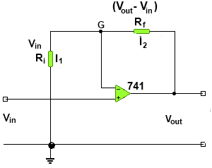
In this figure the current through two resistor is I1 and I2.
The voltage across R1 is Vout and across Rf (Vout – Vout).
I1 = Vin / R1 ------------------(1)
And I2 = (Vout – Vin) / R1 ----------------(2)
Using KCL to point G(virtual ground). We have
I2 + (-I1) = 0
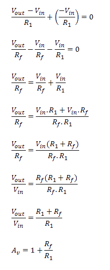
From equation (1) and (2)

