Charged Coupled Devices (CCD): Understanding the Basics
Charged coupled devices (CCD) are an integral part of digital imaging technology. CCDs are electronic image sensors that convert light into digital signals by generating charges through photons. The technology has been in use since the early 1980s and has played a significant role in the development of digital cameras and other image-capturing devices.
The fundamental concept behind CCDs is the use of linked capacitors that transfer electric charges to neighboring capacitors. The external circuit controls the transfer of charges, and each pixel generates an electrical charge proportional to the intensity of light captured by that pixel. CCDs are widely used in digital cameras, video cameras, and other imaging devices because of their ability to capture high-quality images with excellent color accuracy and low noise.
Key Takeaways
- Charged Coupled Devices (CCD) are electronic image sensors that convert light into digital signals.
- CCDs use linked capacitors to transfer electric charges and generate an electrical charge proportional to the intensity of light captured by each pixel.
- CCDs are widely used in digital cameras, video cameras, and other imaging devices because of their ability to capture high-quality images with excellent color accuracy and low noise.
History of Charged Coupled Devices
Charged Coupled Devices (CCD) were invented in 1969 by Willard Boyle and George E. Smith, two physicists at Bell Laboratories. The invention of CCDs came about as a result of the convergence of three important technologies being pursued at that time: magnetic bubbles, MOS semiconductor technology, and the silicon diode array vidicon.
Boyle and Smith's invention of CCDs revolutionized the field of digital imaging. Prior to the invention of CCDs, digital imaging was done using vacuum-tube-based cameras that were bulky, expensive, and difficult to use. CCDs, on the other hand, were much smaller, cheaper, and easier to use, making digital imaging accessible to a wider range of applications.
The first CCD was a 100x100 pixel device that was fabricated in 1970. Over the next few years, CCD technology continued to improve, and by the late 1970s, CCDs were being used in a wide range of applications, including astronomy, medical imaging, and digital photography.
In 2009, Boyle and Smith were awarded the Nobel Prize in Physics for their invention of CCDs. The Nobel Prize committee recognized the impact that CCDs had on digital imaging, stating that "the CCD has become the electronic eye of our time, used in everything from digital cameras to medical imaging equipment to space exploration."
Fundamental Concepts
Principle of Operation
A Charged Coupled Device (CCD) is an electronic component that is used in digital imaging. It is a type of image sensor that converts light into an electrical charge. It consists of an array of capacitors that are linked to each other. The external circuit controls each capacitor, and it can transfer its electric charge to a neighboring capacitor. This process continues until the charge reaches the end of the array, where it is read out and converted into a digital signal.
The principle of operation of a CCD is based on the photoelectric effect. When light falls on a semiconductor material, it excites the electrons in the material, causing them to move from the valence band to the conduction band. This movement of electrons creates a charge, which is proportional to the amount of light falling on the material. In a CCD, this charge is stored in the capacitors, and it is read out at the end of the array.
Types of CCD
There are two types of CCDs: Frame Transfer CCDs and Interline Transfer CCDs.
Frame Transfer CCDs are used in applications where high-quality images are required. They have a separate storage area for the charge, which is read out after the exposure. This type of CCD is used in applications such as astronomy, where high sensitivity is required.
Interline Transfer CCDs have a structure that is similar to a Frame Transfer CCD, but they have a different readout mechanism. They have a row of light-sensitive pixels and a row of masked pixels. The masked pixels are used to transfer the charge from the light-sensitive pixels to the storage area. This type of CCD is used in applications such as digital cameras, where high-speed imaging is required.
In conclusion, CCDs are a major technology used in digital imaging. They convert light into an electrical charge, which is stored in an array of capacitors. There are two types of CCDs: Frame Transfer CCDs and Interline Transfer CCDs. Each type has its own advantages and is used in different applications.
Construction and Design
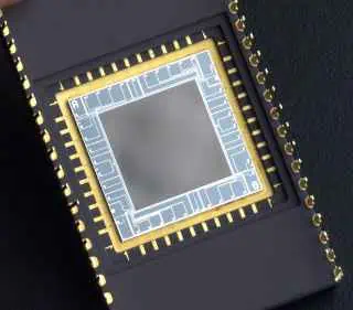
CCDs are solid-state devices that convert light into electrical signals. They are composed of a pixel array, gate structure, and output amplifier.
Pixel Array
The pixel array is the light-sensitive area of the CCD. It is made up of a two-dimensional grid of pixels, each of which contains a photosensitive region and a storage region. The photosensitive region is responsible for converting light into electrical charge, while the storage region holds the charge until it is read out.
Gate Structure
The gate structure controls the transfer of charge between pixels and the output amplifier. It consists of a series of electrodes that are used to create a potential well that traps the charge generated by the photosensitive region. The electrodes are arranged in a four-phase clocking scheme that allows the charge to be transferred from pixel to pixel and ultimately to the output amplifier.
Output Amplifier
The output amplifier reads the charge from the pixel array and converts it into a voltage signal that can be processed by external electronics. It consists of a source-follower circuit that amplifies the voltage signal and a reset transistor that discharges the storage region of each pixel after it has been read out.
Overall, the construction and design of a CCD are optimized for high sensitivity, low noise, and high resolution. The pixel array, gate structure, and output amplifier work together to produce a high-quality image with accurate color reproduction and low image noise.
Applications of Charged Coupled Devices
Charged Coupled Devices (CCDs) are widely used in various applications due to their high sensitivity, low noise, and high resolution. In this section, we will discuss some of the most common applications of CCDs.
Astronomy
CCDs are widely used in astronomy for capturing high-resolution images of celestial objects. They are used in telescopes to capture images of stars, galaxies, and other objects in the night sky. CCDs are preferred over other imaging technologies because they can capture images with high sensitivity and low noise, which is essential for capturing images of faint objects in the night sky.
Microscopy
CCDs are used extensively in microscopy for imaging biological samples. They are used in confocal microscopy, which is a popular technique for studying biological samples. CCDs are preferred over other imaging technologies because they can capture high-resolution images with low noise, which is essential for imaging small biological structures.
Medical Imaging
CCDs are used in medical imaging for capturing high-resolution images of the human body. They are used in X-ray machines, CT scanners, and other medical imaging devices. CCDs are preferred over other imaging technologies because they can capture images with high sensitivity and low noise, which is essential for capturing images of the human body.
Digital Photography
CCDs were the gold standard for camera sensors from the early 80s till the late 2000s. They are used in digital cameras for capturing high-resolution images. CCDs are preferred over other imaging technologies because they can capture images with high sensitivity and low noise, which is essential for capturing high-quality images.
In summary, CCDs are widely used in various applications due to their high sensitivity, low noise, and high resolution. They are preferred over other imaging technologies because they can capture images with high sensitivity and low noise, which is essential for capturing high-quality images.
Advantages and Disadvantages
CCD sensors have been widely used in various applications since their invention in the late 1960s. This section will discuss some of the advantages and disadvantages of using CCDs.
Advantages
- High Image Quality: CCDs have a high sensitivity to light, which makes them capable of producing high-quality images with low noise levels and high dynamic range. This makes them ideal for applications where image quality is critical, such as in scientific research, medical imaging, and surveillance systems.
- Low Dark Current: CCDs have a low dark current, which is the amount of current that flows through the sensor when no light is present. This makes them suitable for long exposure times, as they can capture images with minimal noise.
- Linear Response: CCDs have a linear response to light, which means that the output signal is directly proportional to the amount of light that falls on the sensor. This makes them ideal for applications where accurate measurements are required, such as in spectroscopy and radiometry.
Disadvantages
- Slow Readout Speed: CCDs have a slow readout speed, which limits their use in applications where high-speed imaging is required. CMOS sensors, which have a faster readout speed, have become increasingly popular in recent years due to their ability to capture high-speed images.
- High Power Consumption: CCDs require a high level of power to operate, which can make them unsuitable for battery-powered devices. This is because they require a constant voltage to be applied to the sensor, which can drain the battery quickly.
- Blooming: CCDs can suffer from blooming, which is the spreading of charge from over-exposed pixels to neighboring pixels. This can cause a halo effect around bright objects in the image and can reduce the overall image quality.
Overall, CCDs have many advantages that make them ideal for certain applications, but they also have some limitations that must be considered when choosing a sensor for a particular application.
Future Trends in Charged Coupled Devices
As technology continues to advance, the future of Charged Coupled Devices (CCD) looks promising. Here are some of the trends that are expected to shape the future of CCDs:
Improved Sensitivity
One of the most significant trends in CCD technology is the improvement of their sensitivity. CCDs are already known for their high sensitivity, but advancements in technology are expected to make them even more sensitive. This will allow for better detection of low light levels and more precise measurements.
Higher Resolution
CCDs are widely used in imaging applications, such as digital cameras and telescopes. The future of CCDs is expected to bring even higher resolution, allowing for more detailed images. This will enable scientists to see even further into space and capture more detailed images of the world around us.
Smaller Size
As with most technology, the trend in CCDs is towards smaller and more compact devices. This will allow them to be used in a wider range of applications, including medical imaging and robotics. Smaller CCDs will also enable the development of smaller, more portable devices, such as smartphones with high-quality cameras.
More Efficient Power Consumption
Power consumption is a significant concern for many applications that use CCDs. The future of CCDs is expected to bring more efficient power consumption, reducing the amount of energy needed to operate them. This will make them more environmentally friendly and more cost-effective to use.
Integration with Other Technologies
CCDs are already widely used in a range of applications, but the future is expected to bring even more integration with other technologies. For example, CCDs could be integrated with artificial intelligence to enable more advanced image recognition and analysis. They could also be integrated with other sensors to enable more comprehensive data collection.
Overall, the future of CCDs looks bright. With continued advancements in technology, CCDs are expected to become even more sensitive, higher resolution, smaller, more efficient, and more integrated with other technologies.