Digital To Analog Converter (DAC)
Digital to analog converter is used to convert digital quantity into analog quantity. DAC converter produces an output current of voltage proportional to digital quantity (binary word) applied to its input. Today microcomputers are widely used for industrial control. The output of the microcomputer is a digital quantity. In many applications the digital output of the microcomputer has to be converted into analog quantity which is used for the control of relay, small motor, actuator e.t.c. In communication system digital transmission is faster and convenient but the digital signals have to be converted back to analog signals at the receiving terminal. DAC converters are also used as a part of the circuitry of several ADC converters.
There are several ways of making a digital to analog converter. Some of them are given as under.
- Binary weighted resistor DAC
- R-2R Ladder network
- Serial DAC converter
- BCD DAC
- Bipolar DAC
Binary weighted Resistor DAC
A binary weighted resistor ladder D/A converter is shown in figure 1.

It consists of the following four major components.
- n switches one for each bit applied to the input
- a weighted resistor ladder network, where the resistance are inversely proportional to the numerical significance of the corresponding binary digital
- a reference voltage Vref and
- a summing amplifier that adds the current flowing in the resistive network to develop a signal that is proportional to the digital input.
The behavior of the circuit may be analyzed easily by using "Millman's theorem". It state that "the voltage appearing at any node in a resistive network is equal to the summation of the current entering the node (assuming the node voltage is zero) divided by the summation of the conductance connected to the mode".
Mathematically we can write
Assume that the resistor R1, R2, R3 ....... Rn are binary weighted resistors, thus
R1 = R
R2 = 2R
R3 = 4R
..............
.............
.............
Rn = (2n-1) R
A Resistor Ladder Network, can delivers a binary number say number of n bits.
Each bit controls a switch si that is connected to Vref.
when ai = 1 , then bit is ON, and when ai = 0, then bit is OFF.
The reference voltage source VR is considered to have zero internal impedance. The resistor that are connected to the switches have value such as to make the current flow proportion to the binary weight of the respective input. But the resistor in the MSB position has the value R, the next has the value 2R etc. The resistor of the LSB have the value of
(2n-1) R.
The current flowing in the summing amplifier is
Multiplying and dividing by (2)n-1 R
Above relation shows that output voltage of the D/A converter is proportional to a number represented by the switch that are connected to VR i.e. ai = 1
Maximum current will flow when all ai coefficient are 1, i.e.
When all the bits of digital word have value of 1, then the output current of D/A converter is termed the full scale output current and is an important design parameter.
On the other hand, if all switches are open i.e. all ai coefficients are zero, then the output voltage (current) is zero.
The maximum output voltage Vo = -RiI depends on the feedback resistor Rf. As, the operational amplifier is operated in the negative feedback mode for the purpose of summing so that it performs as an excellent current to voltage converter.
Advantages
As only one resistor is used per it in the resistor network, thus it is an economical D/A converter.
Disadvantages / Limitations
- Resistors used in the network have a wide range of values, so it is very difficult to ensure the absolute accuracy and stability of all the resistors.
- It is very difficult to match the temperature coefficients of all the resistors. This factor is specially important in D/A converters operation over a wide temperature range.
- When n is so large, the resistance corresponding to LBS can assume a large value, which may be comparable with the input resistance of the amplifier. This leads to erroneous results.
- As the switches represent finite impedance that are connected in series with the weighted resistors and their magnitudes and variations have to be taken in to account in a D/A converter design.
R-2R Ladder Network
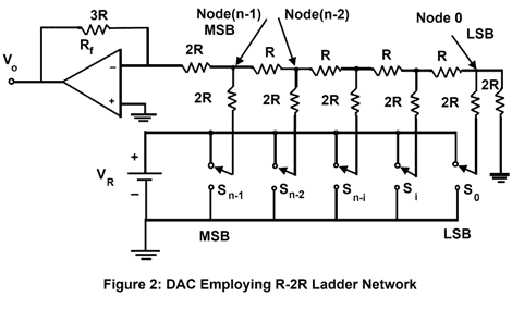
In case of weighted resistor DAC requires a wide range of resistance values and switches for each bit position if high accuracy conversion is required. A digital to analog converter with an R-2R ladder network as shown in figure 2 eliminates these complications at the expense of an additional resistor for each bit.

The operation of R-2R ladder DAC is easily explained considering the weights of the different bits one at a time. This can be followed by superposition to construct analog output corresponding any digital input word. Let only the MSB is turned ON in the first case, and all other bits are OFF, a simplified equivalent circuit can be drawn as shown in figure 3.

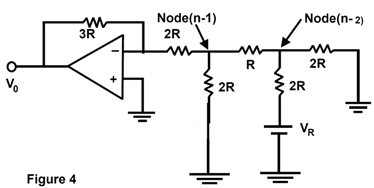
The equivalent circuit with only switch Sn-2 connected to the reference voltage is shown in figure 4.

By using principle of superposition all contributions are summed up and the resultant output is
Vo = VR [an-1 2n-1 + an-2 2n-2 + .............a1 2-(n-1) + ao 2-n]
Vo = VR 2-n [an-1 2n-1 + an-2 2n-2 + .............a1 2+1 + ao 2o]
Note that ai depends on whether th ithe switch is at 0 or at VR. Thus the output of the DAC is proportional to the sum of the weights represented by thosee switches that are connected to VR and the ratio of resistors in the R-2R ladder network.
From this circuit, voltage at mode (n-1) is given by
Vn-1 = VR (R/3R)(-3R) = VR/3
As the input terminal of the operational amplifier is at virtual ground. If the feedback resistor Rf for the operational amplifier is taken as 3R, the corresponding output voltage du to the MSB alone is
Vo = (VR / 3 ) ( -3R / 2R )
= - VR / 2
Let next switch Sn-2 at VR with all other switches at zero. Here, the current at node (n - 2) divide equally to the right and to the left resulting in a voltage at node (n - 2)
Vn-2 = VR / 3
This voltage is attenuated by a factor of 2 at node ( n - 1 ), as
Vn-1 = Vn-2 ( R / 2R) = VR / 6
Output voltage due to node n-2 at the operational amplifier is
Vo = ( VR / 6 ) ( -3R / 2R)
= - VR / 4
Advantages
- Only two values of resistors are used; R and 2R.
- The actual value used for R is relatively less important as long as extremely large values, where stray capacitance enter the picture, are not employs only ratio of resistor values is critical.
- R-2R ladder network are available in monolithic chips,. These are laser trimmed to be within 0.01% of the desired ratios.
- The staircase voltage is more likely to be monotonic as the effect of the MSB resistor is not many times grater than that for LSB resistor.
