Flip Flops
A digital computer needs devices that can store information. A flip-flop is a binary storage device. It can store binary bits either 0 or 1. It has two stable states HIGH and LOW i.e. 1 and 0. It has the property to remain in one state indefinitely until it is directed by an input signal to switch over to the other state. It is also called a bistable multivibrator.
The basic function of the flip-flop is to store data. They can be used to keep a record of the value of a variable (input, output, or intermediate). They are also used to exercise control over the functionality of a digital circuit i.e. change the operation of a circuit depending on the state of one or more flip flops. These devices are mainly used in situations that require one or more of these three. Operations, storage, and sequencing.
Latch Flip Flop
The R-S (Reset Set) flip flop is the simplest of all and easiest to understand. It is basically a device that has two outputs one being the inverse or complement of the other, and two inputs. A pulse on one of the inputs takes on a particular logical state. The outputs will then remain in this state until a similar pulse is applied to the other input. The two inputs are called the Set and Reset inputs (sometimes called the preset and clear inputs).
Such flip flops can be made simply by cross coupling two inverting gates either NAND or NOR gate. Figure 1(a) shows an RS flip flop using the NAND gate and Figure 1(b) shows the same circuit using NOR gate.

To describe the circuit of Figure 1(a), assume that initially both R and S are at the logic 1 state and that output is at the logic 0 state.
Now, if Q = 0 and R = 1, then these are the states of inputs of gate B, therefore the outputs of gate B is at 1 (making it the inverse of Q i.e. 0). The output of gate B is connected to an input of gate A so if S = 1, both inputs of gate A are at the logic 1 state. This means that the output of gate A must be 0 (as was originally specified). In other words, the 0 state at Q is continuously disabling gate B so that any change in R has no effect. Also, the 1 state at Q is continuously enabling gate A so that any change in S will be transmitted through to Q. The above conditions constitute one of the stable states of the device referred to as the Reset state since Q = 0.
Now suppose that the R-S flip flop in the Reset state, and the S input goes to 0. The output of gate A i.e. Q will go to 1 and with Q = 1 and R = 1, the output of gates B Q will go to 0 with Q now 0 gate A is disabled keeping Q at 1. Consequently, when S returns to the 1 state it has no effect on the flip flop whereas a change in R will cause a change in the output of gate B. The above conditions constitute the other stable state of the device, called the Set state since Q = 1. Note that the change of the state of S from 1 to 0 has caused the flip flop to change from the Reset state to the Set state.
There is another input condition that has not yet been considered. That is when both the R and S inputs are at the logic state 0. When this happens both Q and Q will be forced to 1 and will remain so far as long as R and S are kept at 0. However, when both inputs return to 1 there is no way of knowing whether the flip flop will latch in the Reset state or the Set state. The condition is said to be indeterminate because of this indeterminate state great care must be taken when using R-S flip flop to ensure that both inputs are not instructed simultaneously.
| Initial Conditions | Inputs (Pulsed) | Final Output | ||
|---|---|---|---|---|
| Q | S | R | Q | Q |
| 1 | 0 | 0 | indeterminate | |
| 1 | 0 | 1 | 1 | 0 |
| 1 | 1 | 0 | 0 | 1 |
| 1 | 1 | 1 | 1 | 0 |
| 0 | 0 | 0 | indeterminate | |
| 0 | 0 | 1 | 1 | 0 |
| 0 | 1 | 0 | 0 | 1 |
| 0 | 1 | 1 | 0 | 1 |
or more simply shown in Table 2
| S | R | Q |
|---|---|---|
| 0 | 0 | indeterminate |
| 0 | 1 | Set (1) |
| 1 | 0 | Reset(0) |
| 1 | 1 | No Change |
When NOR gates are used the R and S inputs are transposed compared with the NAND version. Also, the stable state when R and S are both 0. A change of state is effected by pulsing the appropriate input to the 1 state. The indeterminate state is now when both R and S are simultaneously at logic 1. Table 3 shows this operation.
| S | R | Q |
|---|---|---|
| 0 | 0 | No Change |
| 0 | 1 | Reset (0) |
| 1 | 0 | Set (1) |
| 1 | 1 | Indeterminate |
Clocked RS Flip Flop
The RS latch flip flop required direct input but no clock. It is very use full to add a clock to control precisely the time at which the flip-flop changes the state of its output.
In the clocked R-S flip flop the appropriate levels applied to their inputs are blocked till the receipt of a pulse from another source called a clock. The flip-flop changes state only when the clock pulse is applied depending upon the inputs. The basic circuit is shown in Figure 2. This circuit is formed by adding two AND gates at inputs to the R-S flip flop. In addition to control inputs Set (S) and Reset (R), there is a clock input (C) also.
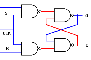
| Initial Conditions | Inputs (Pulsed) | Final Output | Comment | |
|---|---|---|---|---|
| Q | S | R | Q (t + 1) | No Change |
| 0 | 0 | 0 | 0 | No Change |
| 0 | 0 | 1 | 0 | Clear Q |
| 0 | 1 | 0 | 1 | Set Q |
| 0 | 1 | 1 | ??? | indeterminate |
| 1 | 0 | 0 | 1 | No Change |
| 1 | 0 | 1 | 0 | Clear Q |
| 1 | 1 | 0 | 1 | Set Q |
| 1 | 1 | 1 | ??? | indeterminate |
The excitation table for R-S flip flop is very simply derived as given below
| S | R | Q |
|---|---|---|
| 0 | 0 | No Change |
| 0 | 1 | Reset (0) |
| 1 | 0 | Set (1) |
| 1 | 1 | Indeterminate |
D Flip Flop
A D type (Data or delay flip flop) has a single data input in addition to the clock input as shown in Figure 3.
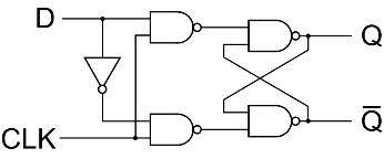
Basically, such type of flip flop is a modification of clocked RS flip flop gates from a basic Latch flip flop, and NOR gates modify it into a clock RS flip flop. The D input goes directly to the S input and its complement through the NOT gate, is applied to the R input.
This kind of flip-flop prevents the value of D from reaching the output until a clock pulse occurs. The action of the circuit is straightforward as follows.
When the clock is low, both AND gates are disabled, therefore D can change values without affecting the value of Q. On the other hand, when the clock is high, both AND gates are enabled. In this case, Q is forced equal to D when the clock again goes low, and Q retains or stores the last value of D. The truth table for such a flip-flop is as given below in Table 6.
| S | R | Q(t + 1) |
|---|---|---|
| 0 | 0 | 0 |
| 0 | 1 | 1 |
| 1 | 0 | 0 |
| 1 | 1 | 1 |
The excitation table for D flip flop is very simply derived given as under.
| S | Q |
|---|---|
| 0 | 0 |
| 1 | 1 |
JK Flip Flop
One of the most useful and versatile flip flops is the JK flip flop the unique features of a JK flip flop are:
- If the J and K input are both at 1 and the clock pulse is applied, then the output will change state, regardless of its previous condition.
- If both J and K inputs are at 0 and the clock pulse is applied there will be no change in the output. There is no indeterminate condition, in the operation of the JK flip flop i.e. it has no ambiguous state. The circuit diagram for this is shown in Figure 4.
When J = 0 and K = 0
These J and K inputs disable the NAND gates, therefore clock signals have no effect on the flip flop. In other words, Q returns its last value.
When J = 0 and K = 1,
The upper NAND gate is disabled the lower NAND gate is enabled if Q is 1 therefore, the flip flop will be reset (Q = 0 , Q =1)if not already in that state.
When J = 1 and K = 0
The lower NAND gate is disabled and the upper NAND gate is enabled if Q is at 1, As a result, we will be able to set the flip flop ( Q = 1, Q= 0) if not already set
When J = 1 and K = 1
If Q = 0 the lower NAND gate is disabled the upper NAND gate is enabled. This will set the flip flop and hence Q will be 1. On the other hand, if Q = 1, the lower NAND gate is enabled and the flip flop will be reset hence Q will be 0. In other words, when J and K are both high, the clock pulses cause the JK flip-flop to toggle. The truth table for the JK flip-flop is shown in Table 8.
| Initial Conditions | Inputs (Pulsed) | Final Output | |
|---|---|---|---|
| Q | S | R | Q (t + 1) |
| 0 | 0 | 0 | 0 |
| 0 | 0 | 1 | 0 |
| 0 | 1 | 0 | 1 |
| 0 | 1 | 1 | 1 |
| 1 | 0 | 0 | 1 |
| 1 | 0 | 1 | 0 |
| 1 | 1 | 0 | 1 |
| 1 | 1 | 1 | 0 |
The excitation table for JK or SR flip flop is very simply derived as given in table 9.
| S | R | Q |
|---|---|---|
| 0 | 0 | No Change |
| 0 | 1 | 0 |
| 1 | 0 | 1 |
| 1 | 1 | Toggle |
T Flip Flop
A method of avoiding the indeterminate state found in the working of RS flip flop is to provide only one input ( the T input ) such, flip flop acts as a toggle switch. Toggle means to change in the previous stage i.e. switch to opposite state. It can be constructed from clocked RS flip flop by incorporating feedback from output to input as shown in Figure 5.
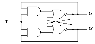
Such a flip-flop is also called a toggle flip-flop. In such a flip flop a train of extremely narrow triggers drives the T input each time one of these triggers, the output of the flip flop changes stage. For instance, Q equals 0 just before the trigger. Then the upper AND gate is enabled and the lower AND gate is disabled. When the trigger arrives, it results in a high S input.
This sets the Q output to 1. When the next trigger appears at point T, the lower AND gate is enabled and the trigger passes through to the R input this forces the flip flop to reset.
Since each incoming trigger is alternately changed into the set and reset inputs the flip-flop toggles. It takes two triggers to produce one cycle of the output waveform. This means the output has half the frequency of the input stated another way, a T flip flop divides the input frequency by two. Thus such a circuit is also called a divide-by-two circuit.
A disadvantage of the toggle flip flop is that the state of the flip flop after a trigger pulse has been applied is only known if the previous state is known. The truth table for a T flip flop is as given Table 7.
| Qn | T | Qn + 1 |
|---|---|---|
| 0 | 0 | 0 |
| 0 | 1 | 1 |
| 1 | 0 | 1 |
| 1 | 1 | 0 |
The excitation table for T flip flop is very simply derived as shown in Table 8.
| T | Q |
|---|---|
| 0 | Qn |
| 1 | Qn |
Generally, T flip-flop ICs are not available. It can be constructed using JK, RS, or D flip flop. Figure 6 shows the relation of the T flip flop using the JK flip flop.
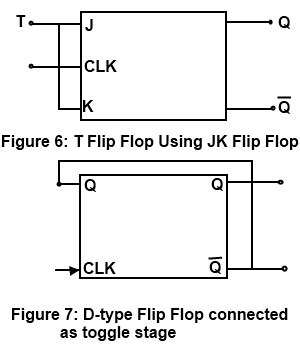
A D-type flip flop may be modified by external connection as a T-type stage as shown in Figure 7. Since the Q logic is used as D-input the opposite of the Q output is transferred into the stage of each clock pulse. Thus the stage having Q - 0 transistors Q= 1, Providing a toggle action, if the stage had Q = 1 the clock pulse would result in Q = 0 being transferred, again providing the toggle operation. The D-type flip flop connected as in Figure 6 will thus operate as a T-type stage, complementing each clock pulse.
Master Slave Flip Flop
Figure 8 shows the schematic diagram of the master-slave J-K flip flop
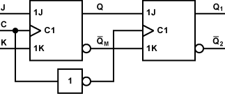
A master-slave flip-flop contains two clocked flip-flops. The first is called a master and the second is a slave. When the clock is high the master is active. The output of the master is set or reset according to the state of the input. As the slave is in active during this period its output remains in the previous state. When the clock becomes low the output of the slave flip-flop changes because it becomes active during the low clock period. The final output of the master-slave flip-flop is the output of the slave flip-flop. So the output of master-slave flip flop is available at the end of a clock pulse.
