Sampling
The signal that is fed to an A/D converter should be maintained constant during the conversion period. In case of an A.C. signal, its instantaneous value is applied to A/D converter and converted into digital quantity. A sample and hold circuit examples the instantaneous value of the A.C. signal and maintains it at a constant level. It makes available this constant voltage for A/D converter which requires a constant input during the conversion period.
Definition
Sampling process converts a continuous signal into a train of pulses. The sampler performing the operation of sampling may be though as a switch which closes for a very short time at discrete periodic instants t = 0, T, 2T, .....kT. Such a sampler is known as periodic or uniform rate sampler with finite sampling pulse width.
Figure 1 illustrates the sampling process in which f(t), a continuous function of time, is converted into a function fv (t) by means of a finite pulse width uniform rate sampler.

Sampling in digital systems can be of many types. For instance, a sampler may have a non-uniform a periodic, cyclic variable or random sampling rate. Also a digital system can have number of samplers with different sampling rates. But in our discussions we shall assume that the sampler is a uniform rate sampler. Further we shall assume that all samplers are synchronized with a signal clock signal. The sampling operation can be interpreted as a modulator with two inputs given as under.
- Input signal
- Carrier consisting of a train of pulses
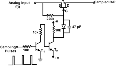
FET Sampling Gate
A sampler circuit using a n-channel FET is shown in figure 2. In the absence of sampling pulse at the input T1 and T2 are OFF and the gate of T3 is at negative potential. Therefore in the absence of an input pulse FET, T3 is OFF and no output is obtained.

A positive pulse at the input of T1 turns it ON which in turn makes T2 and T3 ON. The resistance between drain and source of Q3 becomes very small and f(t) appears at the output for the duration of sampling pulse. The width of sampling pulse is kept small.
Sample and Hold Circuits
A sample and hold circuit in its simplest form is a switch S in series with a capacitor as shown in Figure 3. The switch may be a relay (for very slow waveform), a sampling diode bridge gates a bipolar transistor switch a FET controller by a gating signal voltage.

Figure 3 shows one of the simplest sample and hold circuit. A positive pulse at the gate of the n-channel FET will turn the switch ON and the holding capacitor C will charge the instantaneous value of the input voltage with a time constant (R0 + rDS(ON))C, where R0 is the very small output resistance of the input OP-AMP voltage follower and rDS(ON) is the ON resistance of the FET.
In the absence of a positive pulse, the switch is turned OFF and the capacitor is isolated from any load through the LM 1100 OP-AMP. Thus it will hold the voltage impressed upon it.
The capacitor is charged to the input voltage during the sampling pulse and holds the charge because a high input impedance voltage follower circuit is connected to isolate the capacitor from the output circuit. Therefore, the output remains almost constant at the sampling value till the next sample. The capacitor together with the voltage follower circuit works as a zero order hold circuit.
