Intel 8051 Microcontroller Instruction Types
The 8051 micro-controller instructions are divided among five functional groups:
- Arithmetic
- Logical
- Data transfer
- Boolean variable
- Program branching
1. Arithmetic Instructions
The arithmetic instructions are grouped together in Appendix A. Since four addressing modes are possible, the ADD A instruction can be written in different ways:
ADD A, 7PH (direct addressing)
ADD A, @RO (indirect addressing)
ADD A, R7 (register addressing)
ADD A, #35H (immediate addressing)
All arithmetic instructions execute one machine cycle except the INC DPTR instruction (two machine cycles) and the MUL AB and DIV AB instructions (four machine cycles).
(Note that one machine cycle takes 1 micro sec if the 8051 is operating from a 12 MHz clock.)
The 8051 provides powerful addressing of its internal memory space. Any location can be incremented or decremented using direct addressing without going through the accumulator. For example, if internal RAM location 7FH contains 40H, then the instruction
INC 7FH
Increments this value, leaving 41H in location 7FH.
One of the INC instructions operates on the 16-bit data pointer. Since the data pointer generates 16-bit addresses for external memory, incrementing it in one operation is a useful feature. Unfortunately, a decrement data pointer instruction is not provided and requires a sequence of instructions such as the following:
DEC DPL ; DECREMENT LOW-BYTE OF DPTR
MOV R7, DPL ; MOVE TO R7
CJNE R7, #OFFH, SKIP ; IF UNDERFLOW TO FF
DEC DPH ; DECREMENT HIGH-BYTE TOO
SKIP: (continue)
The high- and low-bytes of the DPTR must be decremented separately; however, the high-byte (DPH) is only decremented if the low-byte (DPL) underflows from 00H to FFH.
The MULAB instruction multiplies the accumulator by the data in the B register and puts the 16-bit product into the concatenated B (high-byte) and accumulator (low-byte) registers. DIV AB divides the accumulator by the data in the B register, leaving the 8-bit quotient in the accumulator and the 8-bit remainder in the B register. For example if A contains 25 (19H) and B contains 6 (06H), the instruction
DIV AB
Divides the content of A by the content of B. The A accumulator is left with the value 4 and B accumulator is left with the value 1. (25 / 6 = 4 with a reminder of 1.)
For BCD (binary-coded decimal) arithmetic, ADD and ADDC must be followed by a DA A (decimal adjust) operation to ensure the result is in range for BCD. Note that DA A will not convert a binary number to BCD; it produces a meaningful result only as the second step in the addition of two BCD bytes. For example, if A contains the BCD value 59 (59H), then the instruction sequence
ADD A, #1
DA A
2. Logical Instructions
The 8051 logical instructions perform Boolean operations (AND, OR, Exclusive OR, and NOT) on bytes of data on a bit-by-bit basis. If the accumulator contains 00110101B, then the following AND logical instruction
ANL A, #01010011B
Leaves the accumulator holding 00010001B. This is illustrated below.
01010011 (immediate data)
AND 00110101 (original value of A)
00010001 (result in A)
Since the addressing modes for the logical instructions are the same as those for arithmetic instructions, the AND logical instruction can take several forms:
ANL A, 55H (Direct addressing)
ANL A, @R0 (Indirect addressing)
ANL A, R6 (Register addressing)
ANL A, #33H (Immediate addressing)
All logical instructions using the accumulator as one of the operands execute in one machine cycle. The others take two machine cycles.
Logical operations can be performed on any byte in the internal data memory space without going through the accumulator. The “XRL direct, #data” instruction offers a quick and easy way to invert port bits, as in
XRL P1, #0FFH
This instruction performs a read-modify-write operation. The eight bits at Port 1 are used; then each bit read is exclusive ORed with the corresponding bit in the immediate data. Since the eight bits of immediate data are all 1s, the effect is to complement each bit read (e.g., A OR 1 = Ᾱ). The result is written back to Port 1.
The rotate instruction (RL A and RR A) shift the accumulator one bit to the left or right. For a left rotation, the MSB rolls into the LSB position. For a right rotation, the LSB rolls into the MSB position. The RLC A and RRC A variations are 9-bit rotates using the accumulator and the carry flag in the PSW. If, for example, the carry flag contains 1 and A contains 00H, then the instruction
RRC A
Leaves the carry flag clear and A equal to 80H. The carry flag rotates into ACC.7 and ACC.0 rotates into the carry flag.
The SWAP A instruction exchanges the high and low nibbles within the accumulator. This is a useful operation BCD manipulation. For example, if the accumulator contains a binary number that is known to be less than 10010, it is quickly converted to BCD as follows:
MOV B, #10
DIV AB
SWAP A
ADD A, B
Dividing the number by 10 in the first two instructions leaves the tens digit in the low nibble of the accumulator, and the ones digit in the B register. The SWAP and ADD instructions move the tens digit to the high nibble of the accumulator, and the ones digit to the low nibble.
3. Data Transfer Instructions
Internal RAM
The instructions that move data within the internal memory spaces execute in either one or two machine cycles. The instruction format
MOV <destination>, <source>
allows data to be transferred between any two internal RAM or SFT locations without going through the accumulator. Remember, the upper 128 bytes of data RAM (8032/8052) are accessed only by indirect addressing, and the SFRs are accessed only by direct addressing.A feature of the MCS-51 TM architecture differing from most microprocessors is that the stack resides in on-chip RAM and grows upward in memory, toward higher memory addresses, The PUSH instruction first increments the stack pointer (SP), then copies the byte into the stack. PUSH and POP use direct addressing to identify the byte being saved or restored, but the stack itself is accessed by indirect addressing using the SP register. This indirect addressing means the stack can use the upper 128 bytes of internal memory on the 8032/8052.
The upper 128 bytes of internal memory are not implemented in the 8031/8051 devices. With these devices, if the SP is advanced above 7FH (127), the PUSHed bytes are lost and the POPed bytes are indeterminate.
Data transfer instructions include a 16-bit MOV to initialize the data pointer (DPTR) in program memory, or for 16-bit external data memory accesses.
The instruction format
XCH A, <source>
causes the accumulator and the addressed byte to exchange data. An exchange “digit” instruction of the form
XCHD A, @Ri
is similar, but only the low-order nibbles are exchanged. For example, if A contains F3H, R1 contains 40H, and internal RAM address 40H contains 5BH, then the instruction
XCHD A, @R1
leaves A containing FBH and internal RAM location 40H containing 53H.
External RAM
The data transfer instructions that move data between internal and external memory use indirect addressing. The indirect address is specified using a 1-byte address (@Ri, where Ri is either R0 or R1 of the selected register bank), or a 2-byte address (@DPTR). The disadvantage in using 16-bit addresses is that all eight bits of Port-2 are used as the high-byte of the address bus. This precludes the use of Port 2 as an I/0 port. On the other hand, 8-bit addresses allow access to a few Kbytes of RAM, without sacrificing all of Port 2. All data transfer instructions that operate on external memory execute in two machine cycles and use the accumulator as either the source or destination operand.
The read and write strobes to external RAM (RD and WR) are activated only during the execution of a MOVX instruction. Normally, these signals are inactive (high), and if external data memory is not used, they are available as dedicated I/O lines.
Look-Up Tables
Two data transfer instructions are available for reading look-up tables in program memory. Since they access program memory, the look-up tables can only be read, not updated. The mnemonic is MOVC for "move content” MOVC uses either the program counter or the data pointer as the base register and the accumulator as the offset.
The instruction
MOVC A, @A+ DPTRcan accommodate a table of 256 entries, numbered 0 through 255. The number of the desired entry is loaded into the accumulator and the data pointer is initialized to the beginning of the table. The instruction
MOVC A, @A+PCworks the same way, except the program counter is the base address. The table is usually accessed through a subroutine. First, the number of the desired entry is loaded into the accumulator, and then the subroutine is called. The setup and call sequence would be coded as follows:
MOV A, #ENTER_NUMBER
CALL LOOK UP
…
…
…
LOOK UP: INC A
MOVC A, @A+PC
RET
TABLE: DB data, data, data, data ...The table immediately follows the RET instruction in program memory. The INC instruction is needed because the PC points to the RET instruction when MOVC executes, Incrementing the accumulator will effectively bypass the RET instruction when the table look-up takes place.
Note however that even though we would expect to get a table of 256 entries when using this technique, we only get 255 entries in this case since we lose one entry due to the effect of the INC A instruction. Consider the entry number of 255 to recycle back to 0 since the accumulator is 8 bit in size. The next instruction, MOVC A, @A + PC, would attempt to load the accumulator with the value of RET, which is invalid. Therefore, valid entries are only from 0 to 254.
4. Boolean Instructions
The 8051 processor contains a complete Boolean processor for single-bit operations. The internal RAM contains 128 addressable bits, and the SFR space supports up to 128 other addressable bits. All port lines are bit-addressable, and each can be treated as a separate single-bit port. The instructions that access these bits are not only conditional branches but also a complete repertoire of move, set, clear, complement. OR, and AND instructions. Such bit operations—one of the most powerful features of the MCS-51TM family of microcontrollers are not easily obtained in other architectures with byte-oriented operations.
The available Boolean instructions are shown in Appendix A. All bit accesses use direct addressing with bit addresses 00H-7FH in the lower 128 locations, and bit addresses 80H–FFH in the SFR space, Those in the lower 128 locations at byte addresses 20H-2FH are numbered sequentially from bit 0 of address 20H (bit 00H) to hit 7 of address 2FH (bit 7FH). Bits may be set or cleared in a single instruction. Single-bit control is common for many I/0 devices, including output to relays, motors, solenoids, status LEDs, buzzers, alarms, loudspeakers, or input from a variety of switches or status indicators. If an alarm is connected to Port 1 bit 7, for example, it might be turned on by setting the port bit
SETB P1. 7
and turned off by clearing the port bit
CLR P1. 7
The assembler will do the necessary conversion of the symbol P1. 7 into the correct bit address, 97H.
Note how easily an internal flag can be moved to a port pin:
MOV C, FLAG
MOV P1. 0, C
In this example, FLAG is the name of any addressable bit in the lower 128 locations or the SFR space. An I/O line (the LSB of Port 1, in this case) is set or cleared, depending on whether the flag bit is 1 or 0.
The carry bit in the program status word (PSW) is used as the single-bit accumulator of the Boolean processor. Bit instructions that refer to the carry bit as "C" assemble as carry specific instructions (e.g., CLR C). The carry bit also has a direct address, since it resides in the PSW register, which is bit-addressable. Like other bit-addressable SFRs, the PSW bits have predefined mnemonics that the assembler will accept in lieu of the bit address. The carry flag mnemonic is "CY," which is defined as bit address 0D7H. Consider the following two instructions:
CLR C
CLR CY
Both have the same effect; however, the former is a 1-byte instruction, whereas the latter is a 2-byte instruction. In the latter case, the second byte is the direct address of the specified bit—the carry flag.
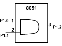
Logical operations such as AND, OR, NAND, NOR, and NOT are easy to implement for single-bit variables. Furthermore, the variables may be input or output variables signal on the 8051’s I/0 ports. Thus, the state of I/0 pin may be directly read or written accompanied by a Boolean operation. Suppose one wanted to compute the logical AND of the input signals on hit 0 and bit 1 of Port 1 and output the result to bit 2 of Port 1.
The following instruction sequence creates this logical operation:
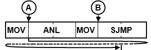
LOOP: MOV C, P1.0 ; n1 = 1 cycle
ANL C, P1.1 ; n2 = 2 cycles
NOV P1.2, C ; n3 = 2 cycles
SJMP LOOP ; n4 = 2 cycles
Bits P1.0 and P1.1 are continuously read with the logical AND of the result continuously presented on P1.2. If the logic operation is implemented using a typical electronic logic circuit, such as a 74AL508, then the input-to-output propagation delay is on the order of 7 ns. This is the time from an input signal transition to the correct logic level appearing at the output. What is the worst case propagation delay for the circuit in figure (a) if implemented using the software above? Figure (b) will assist in answering this question. The worst case scenario is that P1.0 changes just after the first instruction. Shown at “A” in the figure. The change is not sensed until the next pass through the loop. The correct output state appears at “B” in the figure. The solid line in Figure (b) illustrates the sequence of instruction for the worst case scenario. The number of CPU cycles from “A” to “B” following the solid line, is 11 at 12 MHz operation the worst case delay is 11 micro sec. Obviously there is “no contest” in comparing the speed of a micro-controller with speed of electronic logic circuits. The software implementation for figure (a) is about a thousand times slower than a 74LS08 AND gate!
Note that the Boolean instructions include ANL (AND logic) and ORL (OR logic) operations, but not the XRL (exclusive OR logic) operation. An XRL operation is simple to implement, suppose for example, it is required to form the exclusive OR of two bits, BIT1 and BIT2, and leave the result in the carry flag. The instructions are shown below.
MOV C, BIT1
JNB BIT2, SKIP
CPL C
SKIP: (continue)
First, BIT1 is moved to the carry flag. If BIT2 = 0, then C contains the correct result; that is, BIT1 OR BIT2 = 0. If BIT2 = 1. C contains the complement of the correct result. Complementing C completes the operation.
Bit Testing
The code in the example above uses the JNB instruction, one of a series of bit-test instructions that jump if the addressed bit is set (JC, JB, JBC) or if the addressed bit is not set (JNC, JNB). In the above case, if BIT2 = 0 the CPL instruction is skipped. JBC (jump if bit set then clear bit) executes the jump if the addressed bit is set, and also clears the bit; thus, a flag can be tested and cleared in a single instruction.
All PSW bits are directly addressable, so the parity bit or the general purpose flags, for example, are also available for bit-test instructions.
5. Program Branching instructions
There are numerous instructions to control the flow of programs, including those that call and return from subroutines or branch conditionally or unconditionally. These possibilities are enhanced further by the three addressing gram branching instructions.
There are three variations of the JMP instruction: SJMP, LJMP, and AJMP (using the relative, longs and absolute addressing, respectively). Intel's assembler (ASM51) allows the use of generic JMP mnemonic if the programmer does not care which variation is encoded. Assembler from other companies may not offer this feature. The generic JMP assembles to AJMP if the destination contains no forward reference and is within the same 2K page (as the instruction following the AJMP). Otherwise, it assembles to LJMP. The generic CALL instruction (see below) works the same way.
The SJMP instruction specifies the destination address as a relative offset, as shown in the earlier discussion on addressing modes. Since the instruction is two bytes long (an opcode plus a relative offset0, the jump distance is limited to —128 to +127 bytes relative to the address following the SJMP.
The LJMP instruction specifies the destination address as a 16-bit constant. Since the instruction is three byte long (an opcode plus two address bytes), the destination address can be anywhere in the 64K program memory space.
The AJMP instruction specifies the destination address as an 11 bit constant. As with SJMP, this instruction is 2 bytes long, but the encoding is different. The opcode contains three of the 11 address bits, and byte 2 holds the low-order eight bits of the destination address. When the instruction is executed, these 11 bits replace the low-order 11 bits in the PC, and the high-order five bits in the PC stay the same. The destination therefore must be within the same 2K block as the instruction following the AJMP. Since there is 64K of code memory space, there are 32 such block, each beginning at a 2K address boundary (0000H, 0800H, 1000H, !800H, etc., up to F800H.
In all cases the programmer specifies the destination address to the assembler in the usual way as a label or as a 16-bit constant. The assembler will put the destination address into the correct format for the given instruction. If the format required by the instruction will not support the distance to the specified destination address, a “destination out of range” message is given.
Jump tables
The JMP@A + DPTR instruction supports case dependent for jump tables. The destination address is computed at execution time as the sum of the 16-bit DPTR register and the accumulator. Typically the DPTR is loaded with the address of jump table, and the accumulator acts as an index. If, for example, five “cases” are desired, value from 0 through 4 is loaded into the accumulator and jump to the appropriate case is performed as follows.
MOV DPTR, #JUMP_TABLE
MOV A, #INDEX_NUMBER
RL A
JMP @A+DPTRThe RLA instruction above converts the index number (0 through 4) to an even number in the range 0 through 8 because each entry in the jump table is a 2-byte address.
JUMP_TABLE AJMP CASE0
AJMP CASE1
AJMP CASE2
(continue)The CJNE instruction (compare and jump if not equal) is also used for loop control.
Two bytes are specified in the operand field of the instruction, and the jump is executed only if the two bytes are not equal. If, for example, a character has just been read into the accumulator from the serial port and it is desired to jump to an instruction identified by the label TERMINATE if the character is CONTROL-C (03H), then the following instructions could be used:
CJNE A,#031-1,SKIP
SJMP TERMINATE
SKIP: (continue)Since the jump occurs only if A is not equal to CONTROL-C, a skip issued to bypass the terminating jump instruction except when the desired code is read.
Another application of this instruction is in "greater than or "less than comparisons. The two bytes in the operand field are taken as unsigned integers. If the first is less than the second, the carry flag is set. If the first is (greater than or equal to the second, the carry flag is cleared. For example, if it is desired to jump to BIG if the value in the accumulator is greater than or equal to 20H, the following instructions could be used:
CJNE A, #20H, $ + 3
Subroutines and Interrupts
There are two variations of the CALL instruction: ACALL and LCALL, using absolute and long addressing, respectively. As with JMP, the generic CALL mnemonic may be used with Intel's assembler if the programmer does not care which way the address is encoded. Either instruction pushes the content of the program counter on the stack and loads the program counter with the address specified in the instruction. Note that the PC will contain the address of the instruction following the CALL instruction when it gets pushed on the stack. The PC is pushed on the stack low-byte first, high-byte second. The bytes are popped from the stack in the reverse order. For example, if an LCALL instruction is in code memory at locations 1000H-1002H and the SP contains 20H. then LCALL (a) pushes the return address (1003H) on the internal stack, placing 03H in 21H and 10H in 22H; (b) leaves the SP containing 22H; and (c) jumps to the subroutine by loading the PC with the address contained in bytes 2 and 3 of the instruction. The LCALL and ACALL instructions have the same restrictions on the destination address as the LJMP and AJMP instructions just discussed.
Subroutines should end with an RET instruction, which returns execution to the instruction following the CALL. There is nothing magical about the way the RET instruction 1 gets back to the main program. It simply "pops" the last two bytes off the stack and places them in the program counter. It is a cardinal rule of programming with subroutines that they should always be entered with a CALL instruction, and they should always be exited with a RET instruction. Jumping in or out of a subroutine any other way usually fouls up the stack and causes the program to crash.
RET1 is used to return from an interrupt service routine (ISR). The only difference between RET and RET1 is that RET1 signals the interrupt control system that the interrupt in progress is done. If there is no interrupt pending at the time RET1 is executed, then RET1 is functionally identical to RET.
Conditional Jumps
The 8051 offers a variety of conditional jump instructions. All of these specify the destination address using relative addressing and so are limited to a jump distance of —128 to +127 bytes from the instruction following the conditional jump instruction. Note, however, that the user specifies the destination address the same way as with the other jumps, as a label or 16-bit constant, the assembler does the rest. There is no 0-bit in the PSW. The .12 and JNZ instructions test the accumulator data for that condition.
The DJNZ instruction (decrement and jump if not zero) is for loop control. To execute a loop N times, load a counter byte with N and terminate the loop with a DJNZ to the beginning of the loop, as shown below for N = 10
MOV R7, #10
LOOP: (begin loop)
…
…
…
(end loop)
DJNZ R7, LOOP
JNC BIGThe jump destination for CJNE is specified as " $ +3." The dollar sign ($) is a special assembler symbol representing the address of the current instruction. Since CJNE is a 3-byte instruction, "$e +3" is the address of the next instruction, JNC. In other words, the CJNE instruction follows through to the JNC instruction regardless of the result of the compare. The sole purpose of the compare is to set or clear the carry flag. The JNC instruction decides whether or not the jump takes place. This example is one instance in which the 8051 approach to a common programming situation is more awkward than with most microprocessors.