Intel 8085 8-bit Microprocessor
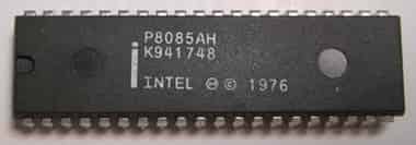
Intel 8085 is an 8-bit, NMOS microprocessor. It is a 40 pin C package fabricated on a single LSI chip. The Intel 8085A uses a single +5V D.C supply for its operation. Its clock speed is about 3 MHz. The clock cycle is of 320 ns. The time for the back cycle of the Intel 8085 A-2 is 200 ns. It has 80 basic instructions and 246 opcodes. Figure 1 shows the block diagram of Intel 8085A. It consists of three main sections, an arithmetic and logic unit a timing and control unit and several registers. These important sections are described as under.
ALU
The arithmetic and logic unit, ALU performs the following arithmetic and logic operations.
- Addition
- Subtraction
- Logical AND
- Logical OR
- Logical EXCLUSIVE OR
- Complement (logical NOT)
- Increment (add 1)
- Decrement (subtract 1)
- Left shift (add input to itself)
- Clear (result is zero)
Timing and Control Unit
The timing and control unit is a section of the CPU. It generates timing and control signals which are necessary for the execution of instructions. It controls provides status, control and timing signals which are required for the operation of memory and I/O devices. It controls the entire operation of the microprocessor and peripherals consented to it. Thus it is seen that control unit of the CPU acts as a brain of the computer.
Registers
Figure 1 show the various registers of Intel 8085A. Registers are small memories within the CPU. They are used by the microprocessor for temporary storage and manipulation of data and instructions. Data remain in the registers till they are sent to the memory or I/O devices. In a large computer the number of registers is more and hence the program requires less transfer of data to and from the memory. In small computers the number of registers is small due to the limited size of the chip. Intel 8085 microprocessor has the following registers.
- One 8-bit accumulator (ACC) i.e. register A.
- Six 8-bit general purpose registers. These are B, C, D, E, H and L.
- One 16-bit program counter, PC.
- Instruction register
- Status register
- Temporary register.

In addition to the above mentioned registers Intel 8085 microprocessor also contains address buffer and data/address buffer. Figure 1 the block diagram of Intel 8085. The program counter PC, contains the address of the next instruction. The CPU fetches an instruction from the memory executes it and increments the content of the program counter. Thus in the next instruction cycle it will fetch next instruction. Instructions are executed sequentially unless an instruction changes the content of the program counter. The instruction register holds the instruction until it is decoded. This cannot be accessed by the programmer.
The stack pointer SP, holds the address of the stack top. The stack is a sequence of memory locations defined by the programmer. The stack is used to save the content of a register during the execution of a program. The last memory location of the occupied portion of the stack is called stack top. For example, suppose that the stack location 2000 is the stack top which is contained by the stack pointer. Now the contents of B-C pair so to be saved. This will be stored in the stack locations 1999 and 1998. The new stack top will be stored in the stack pointer. The new stack top is the location 1998. If more data come they will be stored in the stack location 1997 onwards. Suppose the contents of H-L pair is to be pushed. They will go in 1997 and 1996. The new stack top will be the stack location 1996 and vacant locations are 1995 onward.
There are six 8-bit registers which are used for general purpose as desired by the programmer. These 8-bit registers are A, B, C, D, E, H and L. To handle 16-bit data two 8-bit registers can be combined. The combination of two 8-bit registers is called a register pair. The valid register pairs in Intel 8085 are B-C, D-E and H-L. The H-L pair is used to address memories. The register A is accumulator in Intel 8080/8085. This is for temporary storage used during the execution to a program. It holds one of the operands. The other operand may be either in the memory or in one of the registers.
There is a set of five flip-flops which act as status flags. Each of these flip-flop holds 1-bit flag at indicate certain condition which arises during arithmetic and logic operations. The following status flags have been provided in Intel 8085.
- CARRY (CS)
- ZERO (Z)
- SIGN (S)
- PARITY (P)
- AUXILIARY CARRY (AC)
Carry (CS)
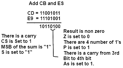
The carry status flag holds carry out of the most significant bit resulting from the execution of an arithmetic operation. If there is a carry from addition or a borrow from subtraction or comparison, the carry flag CS is set to 1, otherwise 0.
Zero (Z)
The zero status flag Z is set to 1 if the result of an arithmetic or logical operation is zero. For non-zero result it is set to 0.
Sign (S)
The sign status flag is set to 1 if the most significant bit of the result of an arithmetic or logical operation is 1 otherwise 0.
Parity (P)
The parity status flag is set to 1 when result of the operation contains even number of 1's. It is set to zero when there is odd number of 1's.
Auxiliary Carry (AC)
The auxiliary carry status flag holds carry out of bit 3 to 4 resulting from the execution of an arithmetic operation.
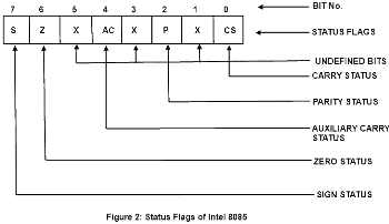
Figure 3 shows the status flags for ADD operation. Take an example of the instruction ADD B. The execution of the instruction ADD B will add the content of the register B to the contents of the accumulator. Suppose the contents of the accumulator and register B are C.B and ES respectively. Now C.B and ES are added and the result is 01, B4. As the accumulator is an 8-bit register B4 remains in the accumulator and there is a carry. The various status flags are shown in figure 2.
PSW
In figure 2 Five bits indicate the five status flags and three bits are undefined. The combination of these 8 bits is called Program Status Word (PSW). PSW and the accumulator are treated as a 16-bit unit for stack operations.
Data and Address Bus
The Intel 8085 is an 8-bit microprocessor. Its data bus is 8-bit wide and hence, 8 bits of data can be transmitted in parallel from or to the microprocessor. The Intel 8085 requires a 16-bits. The 8 most significant bits of the address are transmitted by the address bus, (Pins A8, to A15). The 8 least significant bits of the address are transmitted by address/data bus, (Pins AD0 to AD7). The address/data bus transmits data and address at different moments. At a particular moment it transmits either data or address. Thus the AD-bus operates in time shared mode. This technique is known as multiplexing. First of all 16-bit memory address is transmitted by the microprocessor the 8 MSBs of the address on the A-bus and the 8 LSBs of the address on AD-bus. Thus the effective width of the address is latched so that the complete 16-bit address remains available for further operation. The 8-bit AD-bus now becomes free, and it is available for data transmission 216 (i.e. 64K, where 1K = 1024 bytes) memory location can be addressed directly by Intel 8085. Each memory location contains 1 byte of data.
Timing and Control Signals
The timing and control unit generates timing signals for the execution of instruction and control of peripheral devices. The organization of a microprocessor and types of registers differ from processor to processor. The timing used for the execution of instructions and control of peripherals are different for different microprocessors. The selection of a suitable microprocessor for a particular application is a tough task for an engineer. The knowledge of the organization and timing and control system helps an engineer in the selection of a microprocessor. The design and cost of a processor also depends on the timing structure and register organization.
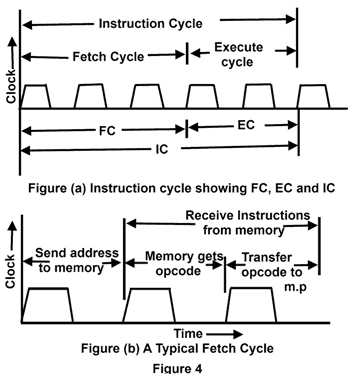
For the execution of an instruction a microprocessor fetches the instruction from the memory and executes it. The time taken for the execution of an instruction is called instruction cycle (IC). An instruction cycle (IC). An instruction cycle consists of a fetch cycle (FC) and an execute cycle (EC). A fetch cycle is the time required for the fetch operation in which the machine code of the instruction (opcode) is fetched from the memory. This time is a fixed slot of time. An execute cycle is of variable width which depends on the instruction to be executed. The total time for the execution is given by
IC = FC + EC
Fetch Operation
In fetch operation the microprocessor gets the 1st byte of the instruction, which is operation code (opcode), from the memory. The program counter keeps the track of address of the next instruction to be executed. In the beginning of the fetch cycle the content of the program counter is sent to the memory. This takes one clock cycle. The memory first reads the opcode. This operation also takes one clock cycle. Then the memory sends the opcode to the microprocessor, which takes one clock period. The total time for fetch operation is the time required for fetching an opcode from the memory. This time is called fetch cycle. Having received the address from the microprocessor the memory takes two clock cycles to respond as explained above. If the memory is slow, it may take more time. In that case the microprocessor has to wait for some time till it receives the opcode from the memory. The time for which the microprocessor waits is called wait cycle. Most of the microprocessor have provision for wait cycles to cope with slow memory.
Execute Operation
The opcode fetched from the memory goes to the data register, DR (data/address buffer in Intel 8085) and then to instruction register, IR. From the instruction register it goes to the decoder circuitry is within the microprocessor. After the instruction is decoded, execution begins. If the operand is in the general purpose registers, execution is immediately performed. The time taken in decoding and the address of the data, some read cycles are also necessary to receive the data from the memory. These read cycle are similar to opcode fetch cycle. The fetch quantities in these cycles are address or data. Figure 4 (a) and Figure 4 (b) shows an instruction and fetch cycle respectively.
Machine Cycle
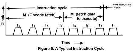
An instruction cycle consists of one or more machine cycles as shown in Figure 5. This figure is for MVI instruction. A machine cycle consists of a number of clock cycles. One clock cycle is known as state.
Applications of Microprocessor
Microprocessor are being used for numerous applications and the list of applications is becoming longer and longer. To give an idea of microprocessor applications few areas are given below.
- Personal Computer
- Numerical Control
- Mobile Phones
- Automobiles
- Bending Machines
- Medical Diagnostic Equipment
- Automatic voice recognizing systems
- Prosthetics
- Traffic light Control
- Entertainment Games
- Digital Signal Processing
- Communication terminals
- Process Control
- Calculators
- Sophisticated Instruments
- Telecommunication Switching Systems
- Automatic Test Systems.
