Class C amplifier operation
A class C amplifier is biased so that it conducts for less than 180° of the input. It will typically have a conduction angle of 90° to 150°. This means that current flows through it in short pulses. The question is "How is a complete signal amplified?" As you will see, a resonant tuned circuit is used for that purpose.
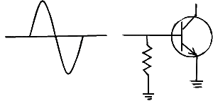
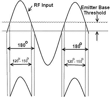
Figure (a) shows one way of biasing a class C amplifier. The base of the transistor simply connected to ground through a resistor. No external bias voltage is applied. An RF signal to be amplified is applied directly to the base. The transistor will conduct on the positive half Cycles of the input wave and will be cut off on the negative half cycles.. Ordinarily, you would think that this would be a class B amplifier. However, this is not the case. Recall that the emitter-base junction of a bipolar transistor has a forward voltage threshold of approximately 0.7V. In other words, the emitter-base junction will not really conduct until the base is more positive than the emitter by + 0.7V. Because of this, the transistor has an inherent built-in bias. When the input signal is applied, the collector current will not flow until the base is positive by 0.7V. This is illustrated in figure. The result is that collector current flows through the transistor in positive pulses for less than the full 180° of the positive alternation.

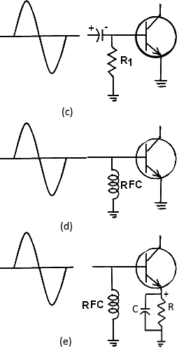
A simple way of supplying bias is with the RC network shown in Fig. (a). Here the signal to be amplified is applied through capacitor CI. When the emitter-base junction conducts on the positive halt cycle, CI will charge to the peak of the applied voltage less the forward drop across the emitter-base junction. On the negative half cycle of the input, the emitter base junction, of course, will be reverse-biased, so the transistor does not conduct during this period of time, however, capacitor C1, will discharge through R1, This produces a negative voltage across R1 which serves as a reverse bias on the transistor. By properly adjusting the time constant of R1 and C1, an average dc reverse bias voltage will be established. The applied voltage will cause the transistor to conduct but only on the peaks. The higher the average dc bias voltage, the narrower the conduction angle and the shorter the duration of the collector current pulses. This method is referred to as signal bias.
Of course, negative bias can also be supplied to a class C amplifier from a fixed dc supply voltage as shown in Fig.(b). After the desired conduction angle is determined, the value of the reverse voltage can be determined. It is applied to the base through the RFC. The incoming signal is then coupled to the base and causes the transistor to conduct only on the peaks of the positive input alternations. This is called external bias but requires a separate negative dc supply.

All class C amplifiers have some form of tuned circuit connected in the collector as shown in Fig.(c). The Primary purpose of this tuned circuit is to form the Complete AC sine wave output. A parallel tuned circuit will ring or oscillate at its resonant frequency whenever it receives a dc pulse. The pulse will charge the capacitor will discharge into the inductor. The Magnetic field in the inductor will increase and then Collapse, causing a voltage to be induced.
Voltage then recharges the capacitor in 0pposite direction. This exchange of energy between the inductor and the capacitor is called the flywheel effect and produces a damped sine-wave at the resonant frequency. If the resonant circuit receives a pulse of current every half cycle, the voltage across the tuned circuit will be a constant amplitude sine-wave at the resonant frequency. Even though the current flows through the transistor in short pulses, the class C amplifier output will be continuous sine Wave.

Modulated class C Amplifier
The transistor amplifier in below Figure is a class C amplifier, as indicated by its bias arrangement. There is no DC supply voltage to the base for biasing. However, the base must be reverse-biased for the transistor to be held in cutoff for more than one-half of the input signal cycle.
The two most common bias arrangements are shown in the inserts. The method shown in figure (a) is used for all low-power transmitters and is called self-bias, signal bias, or base leak bias. The negative dc voltage that holds the base in cutoff is developed by the signal charge across the coupling capacitor CI and is defined by the approximation.
-Vb = -Vpk + 0.7V
A 5 Vpk signal will place the base voltage at —4.3V DC . On the positive peak of the input signal cycle, the coupling capacitor is charged through the base-emitter diode so that the voltage across the capacitor is negative toward the base. The base is negative with respect to the emitter and with respect to ground. On the negative half cycle, the base-emitter diode is reverse biased and the capacitor will discharge through the base resistor Rb, which has a much longer RC time. The base will be held at a negative DC voltage with respect to the emitter.
The disadvantage of self-bias is that if the exciter should fail, the bias will be removed from the final amplifier, and the amplifier may go into very heavy conduction and self-destruct. For this reason, a negative bias supply (-Vbb) is often connected as shown in figure (b). With this arrangement, if the exciter fails, the battery bias will hold the amplifier in cutoff and prevent burnout. Fixed negative DC bias is more common in higher power transmitters.
