Astable Multivibrator
A multivibrator that generates square waves of its own (i.e. without any external trigger pulse) is known as an astable multivibrator. It is also called free ramming multivibrator. It has no stable state but only two quasi-stable (half-stable) makes oscillating continuously between these states. Thus it is just an oscillator since it requires no external pulse for its operation of course it does require DC power.
In such a circuit, neither of the two transistors reaches a stable state. It switches back and forth from one state to the other, remaining in each state for a time determined by circuit constants. In other words, at first one transistor conducts (i.e. ON state), and the other stays in the OFF state for some time. After this period of time, the second transistor is automatically turned ON and the first transistor is turned OFF. Thus the multivibrator will generate a square wave of its own. The width of the square wave and it frequency will depend upon the circuit constants.
Here we like to describe.
- Collector-coupled Astable multivibrator
- Emitter-coupled Astable multivibrator
- Astable multivibrator using OP-AMP
- 555 timer IC as Astable multivibraotor
Collector - Coupled Astable Multivibrator
Figure (a) shows the circuit of a collector-coupled astable multivibrator using two identical NPN transistors Q1and Q2. It is possible to have RL1 = RL2 = RL = R1 = R2 = R and C1 = C2 = C. In that case, the circuit is known as a symmetrical astable multivibrator. The transistor Q1 is forward-biased by the Vcc supply through resistor R2. Similarly the transistor Q2is forward biased by the Vcc supply through resistor R1. The output of transistor Q1is coupled to the input of transistor Q2through the capacitor C2. Similarly, the output of transistor Q2is coupled to the input of transistor Q1 through the capacitor C1.
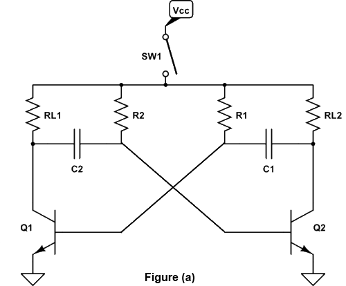
It consists of two common emitter amplifying stages. Each stage provides feedback through a capacitor at the input of the other. Since the amplifying stage introduces a 180o phase shift and another 180o phase shift is introduced by a capacitor, therefore the feedback signal and the circuit works as an oscillator. In other words, because of capacitive coupling none of the transistors can remain permanently out-off or saturated, instead of the circuit has two quasi-stable states (ON and OFF) and it makes periodic transitions between these two states.
The output of an astable multivibrator is available at the collector terminal of either transistor as shown in Figure (a). However, the two outputs are 180o out of phase with each other. Therefore one of the outputs is said to be the complement of the other.
Let us suppose that
- When Q1 is ON, Q2is OFF
- When Q2is ON, Q1is OFF
When the D.C. power supply is switched ON by closing S, one of the transistors will start conducting before the other (or slightly faster than the other). it is so because characteristics of no two similar transistors can be exactly alike suppose that Q1starts conducting before Q2does. The feedback system is such that Q1will be very rapidly driven to saturation and Q2to cut-off. The circuit operation may be explained as follows.
- Since Q1is in saturation whole of VCCdrops across RL1. Hence VC1= 0 and point A is at zero or ground potential.
- Since Q2is in cut-off i.e. it conducts no current, there is no drop across RL2. Hence point B is at VCC.
- Since A is at 0V C2starts to charge through R2towards VCC.
- When the voltage across C2rises sufficiently (i.e. more than 0.7V), it biases Q2 in the forward direction so that it starts conducting and is soon driven to saturation.
- VCC decreases and becomes almost zero when Q2gets saturated. The potential of point B decreases from VCC to almost 0V. This potential decrease (negative swing) is applied to the base of Q1through C1. Consequently, Q1is pulled out of saturation and is soon driven to cut-off.
- Since now point B is at 0V, C1starts charging through R1towards the target voltage VCC.
- When the voltage of C1increases sufficiently. Q1becomes forward-biased and starts conducting. In this way, the whole cycle is repeated.
It is observed that the circuit alternates between a state in which Q1is ON and Q2is OFF and the state in which Q1is OFF and Q2is ON. This time in each state depends on RC values. Since each transistor is driven alternately into saturation and cut-off. The voltage waveform at either collector (points A and B in Figure (b) is essentially a square waveform with a peak amplitude equal to VCC.
Emitter - Coupled Astable Multivibrator
Figure (b) shows the circuit diagram of an emitter-coupled asable multivibrator.
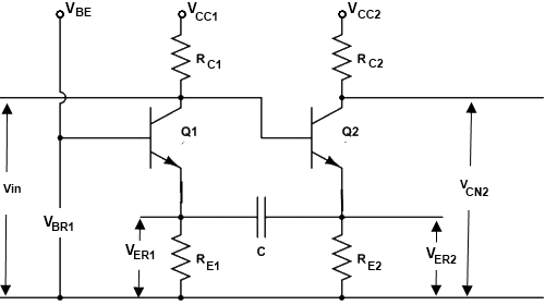
In a collector-coupled symmetrical astable multivibrator if it is desired to vary the frequency., then it is necessary
- to vary both the timing capacitor simultaneously
- to vary the timing resistor subject to the conduction that the values are enough to keep the transistors in saturation
- to vary VBBwhich also can not be varied over a long range. Thus it is difficult to achieve frequency control in collector coupled astable multivibrator, not an emitter-coupled multivibrator, to be described here, which has a single timing capacitor connected across the emitter. This capacitor can be varied easily.
In order to explain the operation of the circuit, it is necessary that the following conditions must be satisfied.
- In D.C. conduction i.e. with timing capacitor C removed bias should be so adjusted that both the transistors are in the active region.
- Under the D.C. conditions, the D.C. loop gain should be less than unity to void the bistable operation.
- In the active region, the loop gain must be greater than unity at some non-zero frequency.
- Bias conditions are so adjusted that with capacitor C concerned, during normal operation, transistor C1operates between cut-off and saturation while transistor C2operates at the same time between its active region and the off region. This transistor Q1operates in saturated mode and transistor Q1operates in saturated mode and transistor Q2operates in unsaturated mode.
Astable multivibrator using OP-AMP
Figure (c) shows a differential input operational amplifier acting as a free-running symmetrical multivibrator.
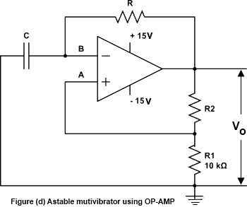
The two states of the circuit between which it switches are those in which the amplifier output is at positive and negative saturation. R1and R2provide a fixed level of positive feedback and R and C provide a frequency-dependent level of negative feedback. At high frequencies, the negative feedback is reduced and the circuit becomes unstable. The circuit can not hang up in either output stage and is self-starting.
As terminal B is positive with respect to terminal A and its potential is decreasing as C charges down through R. When the potential difference between the two input terminals approached zero the amplifier comes out of saturation. The positive feedback from the output to terminal A causes a regenerative switching which drives the amplifier to positive saturation. The voltage across a capacitor in series with a resistor can not change instantaneously, the potential at the terminal B, therefore, remains substantially constant during this rapid transition. Capacitor C now charges up through R and the potential at C rises exponentially when it reaches βV01 (sat) the circuit switches back to the state in which the amplifier is in negative saturation.
555 Timer Circuit as a Astable Multivibrator
Figure (d) shows the circuit diagram of an astable multivibrator using a 555 timer.
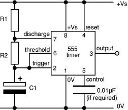
Astable Operation
The figure shows an astable mode of operation for the 555 timer. Here, the capacitor C will charge through RA and RS then discharge through RS only. The duty cycle may be controlled, therefore, by the values of RA and RS.
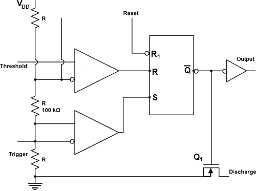
In order to understand the operation of both astable and monostable multivibrator circuits using a 555 timer, a functional diagram of a 555 timer is shown in Figure (e).