Thyristor
Thyristor was invented in 1957 at Bell Labs. They are extensively used as switches, operating from conducting state to non-conducting state. Basically, they are the rectifiers with a control element.
Construction
They are four layer or PNPN devices. Thyristor consists of four alternately doped semiconductor layers. They form three functions which are named. J1, J2 and J3.
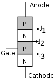
External leads are attached to only three layers out of four they are called anode, cathode and gate. Anode is attached to the outer P-layer cathode is attached to the outer N-layer while the gate is attached to the inner P-layer.
Symbolic Representation
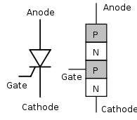
A thyristor is usually represented by the schematic symbol as shown. This symbol actually resembles to that of a diode but with gate.
Two transistors Analogy
The operation of a thyristor can be best understood by considering its two transistor analogy
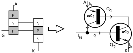
The thyristor is split into two three layer transistors. Q1 is a PNP transistor while Q2 is an NPN transistor. It should also be noted that the collector of Q1 is also the base current of Q2 and the base current of Q1 is also the collector current of Q2.
Operation
Thyristor two transistor circuits will start conducting if the emitter base function of both the transistors is forward biased. If the anode is made positive with respect to the cathode, the thyristor will not conduct. It is because the gate is open and the emitter base function of the NPN transistor is not subjected to forward bias and hence, there is no base current for NPN transistor. Therefore, transistor Q2 is cutoff. Thus Q2 transistor will not allow a base current to flow through the emitter junction of the PNP (Q1) transistor and hence Q1 transistor is also cut off or non-conducting state.
Now it the gate of the equivalent circuit model is momentarily made positive with respect to the cathode, the emitter base junction of NPN (Q2) will become forward biased & it will conduct. This will cause the base current to flow through the PNP (Q1) transistor & it will also conduct.
However, the collector current of PNP (Q1) transistor will now cause the base current to flow through the NPN (Q2) transistor. Hence, the two transistors hold each other in the “ON” or conducting state allowing the current to flow from anode to cathode.
Calculation for The Anode Current
Let
α1 = IC1/IE1 = Current gain of Q1
α2 = IC2/IE2 = Current gain of Q2
ICBO1 = Leakage current for Q1
ICBO2 = Leakage current for Q2
Now
IC1 = α1 IE1 + ICBO1 As IE1 = IA
so
IC1 = α1 IA + ICBO1------------------- Eq. 1
Similarly
IC2 = α2 IE2 + ICBO2 As IE2 = IK
IC2 = α2 IK + ICBO2 -------------------- Eq. 2
Now Combining Eq. 2 & 1
IC1 + IC2 = α1 IA + ICBO1 + α2 IK + ICBO2 ----------------------Eq. 3
Consider Transistor Q1
IA = IB1 + IC1
= IC2 + IC1
∴ Eq. 3 becomes
IA = α1 IA + ICBO1 + α2 IK + ICBO2 -----------------------Eq. 4
By the application of Gate current "IG"
IG1 + IC1 = IB2 -------------------Eq. 5
Now, for transistor Q2
IK = IB2 + IC2 ∴ IB2 = IG + IC1
∴ IK = IG + IC1 + IC2
From relation (A)
IK = IA + IG
Using this value in Eq. 4
IA = α1 IA + ICBO1 + α2(IA + IG)+ ICBO2
IA - IA(α1 + α2) = α2 IG + ICBO1+ ICBO2
=> IA = (α2 IG + ICBO1+ ICBO2)/( I(α1 + α2)) ------------------- Eq. 6
Where α1 + α2 = G1 = loop gain
While "α1" varies with emitter current IE1 = IA & "α2" varies with the emitter current IK = IA + IG.
The increase in α1 & α2 would further increase IA. Therefore there is a regenerative or positive feedback effect.
If (α1 + α2 ) tends to be unity, the denominator of Eq. 6 approaches zero, resulting in a large value of anode current "IA" & the thyristor will turn on with a small gate current.
Asymmetrical Thyristor
To reduce the time taken by thyristor to recover its blocking state after turn off, the silicon is made thinner. This is achieved at the expense of reverse blocking ability of thyristor. Such a device is called asymmetrical thyristor. In applications where reverse blocking capability is of little importance, the switching time is reduced to a few microseconds compared ot tens of microseconds for conventional thyristor.
How to Turn Thyristor OFF
To turn off the thyristor the anode current must be reduced below the holding level and a relatively long time allowed elapsing for the thyristor to recover its blocking state before a forward voltage can again be applied without conduction.
More typically to turn off the thyristor, the anode current is driven in reverse by external circuitry.
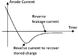
The reverse current flows for a very short duration permitting charges movement within PN layers allowing further reverse current after the storage charge has been removed the central control junction will however not block the reapplication of forward voltage until a further time has elapsed. Typically 10 to 100µs must elapse before the forward voltage can again be applied without breakdown. The charge could be 20µs for a 20A thyristor.
Thyristor gating requirements
The gate cathode characteristics of thyristors vary in a considerable range within a given production batch.
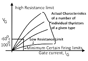
All thyristors can be assumed to have a characteristic curve lying somewhere between high and low resistance limit. The minimum level of current and voltage required to turn on the thyristor is a function of the junction temperature, and indication of these minimum levels is shown.
The current into and voltage at the gate are both subject to maximum values also exceed certain minimum levels. The product of gate voltage and current gives a power level to which a maximum is set.
